鑫景福致力于滿足“快速服務,零缺陷,輔助研發”PCBA訂購單需求。


PCB制造
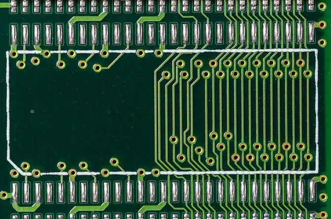
PCB production process flow 1
There are many kinds of PCB production process flow charts. According to the number of layers of the circuit board and the production process of the circuit board, they are divided into: double-sided circuit board process, multi-layer circuit board process, PCB copper electroplating process, CNC lathe processing process, PCB circuit graphICs transfer and contour processing. The production process flow chart and CAM aided design are described in detail below.
Basic manufacturing process flow of PCB produced in the factory
printed boards can be divided into single-sided, double-sided and multi-layer printed boards according to the number of layers of conductor patterns. The basic manufacturing process of single panel is as follows:
Foil clad plate -->blanking -->baking plate (to prevent deformation) -->mold making -->cleaning and drying -->film pasting (or screen printing) -->exposure development (or anti-corrosion ink) -->etching -->film removal -->electrical continuity detection -->cleaning -->screen printing solder mask (printing green oil) -->curing -->screen printing MARK number -->curing -->drilling -->shape processing -->cleaning and drying -->inspection -->packaging -->finished products.
The basic manufacturing process of double-sided plate is as follows:
In recent years, the typical processes for manufacturing double-sided hole metallized PCB are SMOBC method and pattern electroplating method. The process wire method is also used in some specific occasions.
1. Graphic electroplating process flow
Foil clad plate -->blanking -->punching and drilling reference hole -->numerical control drilling -->inspection -->deburring -->chEMIcal plating thin copper -->electroplating thin copper -->inspection -->brushing -->film pasting (or screen printing) -->exposure development (or curing) -->inspection and repair -- -->graphic electroplating (Cn+Sn/Pb) -->Film removal -->etching -->inspection and repair -->nickel plating and gold plating on the plug -->hot melt cleaning -->electrical on-off detection -->cleaning -->screen printing solder resistance figure -->curing -->screen printing mark symbol -->curing -->contour processing -->cleaning and drying -->inspection -->packaging -->finished products.
In the process, the two processes of "electroless thin copper plating -->thin copper plating" can be replaced by the one of "electroless thick copper plating", both of which have advantages and disadvantages. Pattern electroplating - etching method of double hole metallized plate is a typical process in the 1960s and 1970s. In the 1980s, the bare copper coating resistance welding film process (SMOBC) was gradually developed, especially in the manufacturing of precision double panel.
2. Bare copper coating resistance welding film (SMOBC) process
The main advantage of the SMOBC board is to solve the solder bridge short circuit between thin lines. At the same time, due to the constant lead tin ratio, it has better solderability and storage than the hot melt board.
There are many methods to manufacture SMOBC board, including standard pattern electroplating subtraction method and lead tin stripping SMOBC process; Substitute tin plating or tin DIPping for the subtractive graphic electroplating SMOBC process of electroplating lead and tin; Plugging or masking hole method SMOBC process; Additive SMOBC process, etc. The following mainly introduces the SMOBC process of pattern electroplating followed by lead and tin stripping and the SMOBC process of hole plugging.
The SMOBC process of pattern electroplating and lead tin stripping is SIMilar to the pattern electroplating process. Changes occur only after etching.
Double sided copper clad foil -->from graphic electroplating process to etching process -->lead and tin removal -->inspection -->cleaning -->solder mask -->nickel and gold plating on plug -->adhesive tape on plug -->hot air leveling -->cleaning -->screen printing mark symbol -->contour processing -->cleaning and drying -->finished product inspection -->packaging -->finished product.
Film backplane is the leading process of PCB production, and the quality of film backplane directly affects the production quality of PCB. When producing a certain kind of printed circuit board, there must be at least one set of corresponding film base plate. Each conductive pattern (signal layer circuit pattern and ground and power layer pattern) and non-conductive pattern (solder mask pattern and character) of the printed board shall have at least one film negative. Through photochemical transfer process, various patterns are transferred to production plates.
The use of film base in PCB production is as follows:
Photosensitive mask patterns in pattern transfer include circuit patterns and photoresist patterns.
Screen printing process in the production of screen templates, including solder mask graphics and characters.
Machining (drilling and contour milling) CNC machine tool programming basis and drilling reference.
With the development of electronic industry, the requirement of printed circuit board is higher and higher. The high density, thin wire and SMAll aperture of PCB design are becoming faster and faster, and the production process of PCB is becoming more and more perfect. In this case, if there is no high-quality film base plate, high-quality printed circuit boards can be produced. Modern printed board production requires that the film base should meet the following conditions:
The dimensional accuracy of the film base must be consistent with the accuracy required by the printed board, and the deviation caused by the production process should be taken into account for compensation.
The graphics of the film base shall meet the design requirements, and the graphic symbols shall be complete.
The graphic edges of the film base plate are straight and neat, without blurring; The contrast between black and white is large, meeting the requirements of photosensitive technology.
The material of film base plate shall have good dimensional stability, that is, small dimensional change due to changes in ambient temperature and humidity.
For the film base plate of double-sided plate and multilayer plate, it is required that the overlap accuracy of bonding pad and public figure is good.
Each layer of the film base shall be clearly marked or named.
The film substrate can pass through the required wavelength of light, and the wavelength range required for general photosensitivity is 3000-4000A.
In the past, when making a film base, it was generally necessary to make a photographic base first, and then use photography or reproduction to complete the production of the film base. This year, with the rapid development of computer technology, the production process of film plate has also made great progress. The use of advanced laser photo drawing technology has greatly improved the production speed and the quality of the bottom plate, and can produce high-precision, thin wire graphics that could not be completed in the past, making the CAM technology of PCB production more perfect
Copper Clad Laminates (CCL for short), referred to as copper clad laminates or copper clad laminates, are the substrate materials for manufacturing printed circuit boards (hereinafter referred to as PCBs). At present, the PCB made by the most widely used etching method is selectively etched on the copper clad foil to obtain the required circuit graphics. Copper clad laminate is mainly responsible for conducting, insulating and supporting the entire printed circuit board. The performance, quality and manufacturing cost of printed circuit board depend on copper clad foil to a large extent.
The main process flow of hole plugging method is as follows:
Double sided foil clad plate -->drilling -->electroless copper plating -->whole plate copper plating -->hole plugging -->screen printing imaging (positive image) -->etching -->screen printing material removal, hole plugging material removal -->cleaning -->solder resistance figure -->plug nickel plating, gold plating -->plug adhesive tape -->hot air leveling -->the following process is the same as above to the finished product.
The process steps of this process are relatively simple, and the key is to block holes and clean the ink that blocks holes.
In the hole blocking process, if a special masking type dry film is used to cover the holes instead of using the hole blocking ink to block the holes and screen printing imaging, and then the holes are exposed to make positive images, this is the mask hole process. Compared with the hole plugging method, it no longer has the problem of cleaning the ink in the hole, but has higher requirements for masking the dry film.
The foundation of the SMOBC process is to first produce the bare copper hole metallized double-sided plate, and then apply the hot air leveling process.

PCB production process flow 2
10-30,2022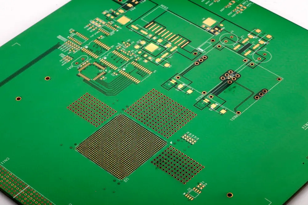


抖音二維碼

Q Q二維碼

微信二維碼
點擊
然后
聯系
然后
聯系
電話熱線
13410863085Q Q

微信

- 郵箱