鑫景福致力于滿足“快速服務,零缺陷,輔助研發”PCBA訂購單需求。


PCB制造
General Steps of PCB Process Drawing
Each time a PCB is designed, the following sequence should be followed to save time and get the best results.
1. Select the name of SCH, PCB and other files (in English, numbers), and add the extension.
2. SchematIC diagram
First, design the grid size and drawing size, select metric system, and add library components. Draw the diagram according to the circuit function module. The drawing method of components and lines should make it easy to see the principle clearly. Try to be even and beautiful. Do not route wires inside the components. Be careful not to route wires in the middle of the pins, because there is no electrical connection. It is better not to connect two component pins directly. After drawing, it can be numbered automatically (except for special requirements), and then add the corresponding nominal value. It is better to change the nominal value to red and bold, so that it can be distinguished from the label. It is better to put the label and nominal value in the appropriate position. Generally, the left side is the label, the right side is the nominal value, or the upper side is the label, and the lower side has no nominal value. Habitually save in the process! First, make sure that the schematic diagram is completely correct, perform ERC check, and then print and check. Secondly, it is better to understand the circuit principle, for high and low voltage; Large and SMAll current; Analog, digital; Large and small signals; The power is divided into small and large blocks for the convenience of later layout.
3. Make PCB component library
For the production of component packages that are not in the standard library and your own common library, pay attention to drawing the top view, size, pad size, location, number, hole size, direction, (printing method is used to measure the size). The name shall be in English, and it is better to read it easily. It is better to MARK the corresponding size so that it can be searched next time (it can be saved in the form of a table corresponding to the name and the corresponding size). For commonly used diodes, attention should be paid to the marking method of triodes. It is better to have commonly used series of diodes and triodes packaged in your own library, such as 9011-90181815, D880, etc. For LED, RAD0.1, RB.1/ 2. Component packages that are commonly used but not in the standard library should be in their own library. You should be familiar with the sealing form of common components (resistance, capacitor, diode, triode).
4. Generate Network Table
Encapsulate, save, ERC check and generate component list check in schematic diagram. Generate a network table.
5. Create PCB
Select the metric system, capture and visible grid size, design the outer frame (guide or draw by yourself) as required, and then place the location of the fixing hole. The size (3.5mm inner hole pad can be used for 3.0mm screws, and 3 inner holes can be used for 2.5 screws), and change the pad at the edge first, with the hole size and location fixed. Add the required library.
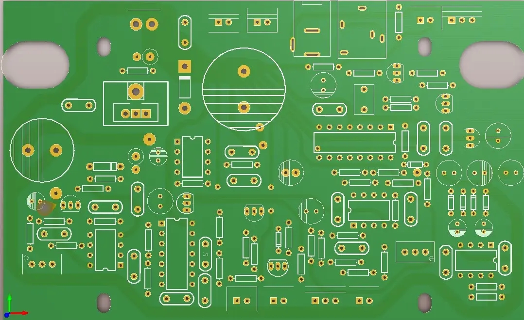
6. Layout
Call the network table, import components, modify the size of some pads, set the routing rules, and change the size, thickness, and hidden nominal value of the label. Then place and lock the components that need special positions. Then, according to the functional module layout (you can select the mode of transition from SCH to PCB), the components are generally not flipped with X and Y, but with space rotation or L key (because some components cannot be flipped, such as integrated blocks, relays, etc.). For a function module, place the central component or large component first, and then place the small component beside it. (For example, first place the manifold block, and then place the components directly connected to two pins of the manifold block, and then place the components connected to one pin of the manifold block. SIMilar components should be placed together as much as possible, and the convenience of wiring should also be considered if they are beautiful.). Of course, some special components should be placed first, such as some filter capacitors and crystal oscillators. There are also components that will interfere. The overall consideration is to stay away from them. The high and low voltage modules shall be spaced at least 6.4mm apart. Attention shall be paid to the location of heat sink, connector and fixing frame. FILL can be used in some places that cannot be wired. Also consider heat dissipation and thermal elements. The placement of resistors and diodes: horizontal and vertical.
(1) Horizontal placement: When the number of circuit components is small and the size of the circuit board is large, it is generally better to use horizontal placement; When the resistance below 1/4W is placed horizontally, the distance between two pads is generally 4/10 inches, and when the resistance below 1/2W is placed horizontally, the distance between two pads is generally 5/10 inches; When the diode is laid horizontally, 1N400X series rectifier tube is generally 3/10 inch; 1N540X series rectifier tube, generally 4~5/10 inches.
(2) Vertical placement: When the number of circuit components is large and the size of the circuit board is small, vertical placement is generally adopted. The spacing between two pads is generally 1~2/10 inches.
7. Wiring
First, set the content in the rule. The wide points (0.5mm-1.5mm) that can be set for VCC, GND high-power and other high current lines. Generally, 1mm can pass 1A current. Large points can be set for large voltage line spacing, generally 1000 V for 1mm. After setting, some important wires such as VCC and GND should be laid first. Pay attention to the differentiation of each module. It is better to add some lines to the single panel. The vias are not necessarily horizontal and vertical. Generally, the bonding pads of the integrated block are not wired. Wide lines with high current can be drawn on the solder layer for tin coating; 45 ° angle for wiring
8. Modify line manually
Modify the width, corner, tear patch or bonding pad of some lines (required for single panel), lay copper, and handle the ground wire.
9. Inspection
DRC, EMC, etc. can be checked, and then printed for checking and network table comparison. Component list check.
10. Add model (generally made of wire MESh)
11. The potentiometer is generally adjusted clockwise to increase (voltage, current, etc.)
12. High frequency (>20MHz) is generally grounded at multiple points< 10MHz or<1MHz single point grounding. The grounding is mixed.
13. As required, not all devices should be packaged according to the standard, which can be jumper or vertical welding.
14. When wiring the printed circuit board, the circuit board manufacturer shall first determine the position of components on the board, and then lay the ground wire and power wire. When arranging high-speed signal lines, it is better to consider low-speed signal lines. The positions of the elements are grouped according to the power supply voltage, digital simulation, speed and current. Under safe conditions, the power cord should be as close to the ground as possible. Reducing the loop area of differential radiation is also helpful to reduce the circuit crosstalk. When it is necessary to arrange fast, medium and low speed logic circuits on the circuit board, the high-speed logic circuits shall be placed close to the edge connector, while the low-speed logic circuits and memories shall be placed far away from the connector. This is beneficial to the reduction of common impedance coupling, radiation and crosstalk. Grounding is the most important. At most times, you need to back up, or some steps are easy to crash, and you need to back up files when they are damaged.


抖音二維碼

Q Q二維碼

微信二維碼
點擊
然后
聯系
然后
聯系
電話熱線
13410863085Q Q

微信

- 郵箱