鑫景福致力于滿足“快速服務,零缺陷,輔助研發”PCBA訂購單需求。


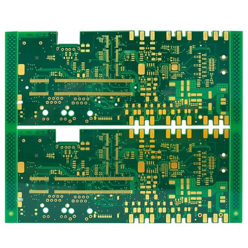
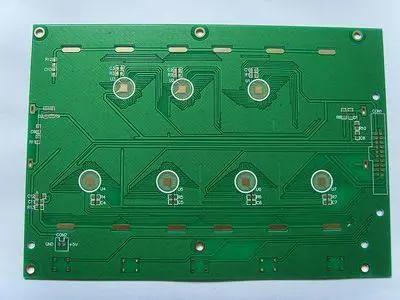
PCB制造
PCB factory: What are the precautions for PCB proofing?
As an engineer group, precautions for proofing include:
1. Carefully select the proofing quantity to effectively control the cost.
2. Specially confirm the devICe packaging to avoid the failure of proofing due to packaging errors.
3. Carry out a comprehensive electrical inspection to improve the electrical performance of the PCB board.
4. Do a good job of signal integrity layout, reduce noise and improve PCB stability.
As the manufacturer of four layer board proofing, the following precautions for proofing:
1. Carefully check PCB documents to avoid data problems.
2. Carry out overall process approval and process configuration with the manufacturer.
3. Control production quantity, reduce cost and maintain quality.
4. Communicate with the proofing customer on precautions to prevent accidents in advance.
The above is just a brief explanation. Next, we will introduce the specific details for you in detail, hoping to be helpful to relevant netizens.
1. Make Physical Border
The closed physical frame is a basic platform for future component layout and routing, and also a constraint for automatic layout. Otherwise, the components coming from the schematic diagram will be at a loss. But you must pay attention to the accuracy here, otherwise you will have a lot of trouble in the future. Also, it is better to use arc at the corner, which can avoid sharp corner scratching workers on the one hand and reduce the stress effect on the other. In the past, one of my products was always broken in the process of transportation by a few machines. It would be better to use circular arc instead.
2. Introduction of components and networks
It should be easy to draw components and networks into the drawn border, but problems often occur here. Be careful to solve the problems one by one according to the prompted errors, otherwise it will take more effort later. The problems here are generally as follows: the package form of the component cannot be found, the component network problem, and there are unused components or pins. These problems can be solved quickly according to the prompts. PCB proofing
The layout and routing of components have a great impact on the life, stability and electromagnetic compatibility of products, which should be paid special attention to. Generally speaking, the following principles should be followed:
4. Placement order
First place the components at fixed positions related to the structure, such as power sockets, indicator lights, switches, connectors, etc. After placing these components, use the LOCK function of the software to lock them, so that they will not be moved by mistake in the future. Then place special components and large components on the circuit, such as heating components, transformers, ICs, etc. Finally, place the SMAll device.
5. Pay attention to heat dissipation
Special attention shall be paid to heat dissipation in component layout. For high-power circuits, those heating elements such as power tubes and transformers should be placed as far away as possible to facilitate heat EMIssion. They should not be concentrated in one place, nor should high capacitors be too close to avoid premature aging of electrolyte. The schematIC design before single panel proofing is a preliminary preparation. When drawing the schematic, pay attention to the connection of each file as a whole in the hierarchical design, which is also important for future work. Due to the difference of software, some software may appear to be connected but not actually connected (in terms of electrical performance). If you do not use the relevant detection tools to detect, in case of a problem, it will be late to find out when the board is ready. Therefore, we have repeatedly stressed the importance of doing things in order and hope to draw everyone's attention.
The circuit board manufacturer and circuit board designer will explain to you the precautions for PCB proofing.


抖音二維碼

Q Q二維碼

微信二維碼
點擊
然后
聯系
然后
聯系
電話熱線
13410863085Q Q

微信

- 郵箱