鑫景福致力于滿足“快速服務(wù),零缺陷,輔助研發(fā)”PCBA訂購單需求。


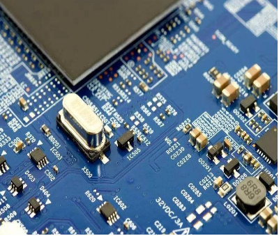
PCB制造
What problems should be paid attention to when using PCB components for PCB proofing
In, on the prEMIse of meeting the functional requirements of the circuit, PCB components with high sensitive voltage threshold should be used as far as possible. Because the electrostatIC and discharge sensitivity of a circuit board depends on the component with the lowest sensitive voltage threshold in the circuit board.
1. Limiting the output current can avoid the locking effect of CMOS circuit
Lock in effect refers to the existence of parasitic PNP transistors and NPN transistors in the internal structure of CMOS circuits, and a parasitic PNPN silicon controlLED structure is formed between them. The positive feedback structure of this interlock may be triggered by external factors (such as electrostatic discharge), which will flow current on the PNP tube (or NPN tube), and then pass through another
parasitic NPN tube (or PNP tube) to amplify the current, and the current will become larger and larger due to the positive feedback effect and eventually burn out. It can be seen that limiting the current so that it cannot reach the level of maintaining the locked state is one of the issues to be considered for CMOS devices during PCB proofing.
The common solution is to use a resistor to separate each output terminal from its cable, and use two high-speed switching diodes to clamp to VDD (drain power supply) and VSS (source power supply) with cable.
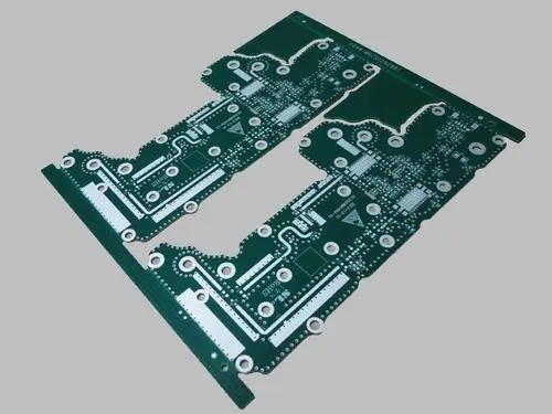
PCB proofing
2. Use filter network
Long input cables are sometiMES required between CMOS circuit system and mechanical contacts, which increases the possibility of electromagnetic interference. Therefore, filter network should be considered. At the same time, long input lines must be accompanied by large distributed capacitance and inductance, which is easy to form LC self-excited oscillation, leading to diode burning of the protection network. The solution is to connect a PCB resistor in series at the input end. The resistance value can be selected according to the formula R=VDD/1mA.
3. RC network
Where feasible, for sensitive inputs of bipolar PCB devices, RC network composed of resistors with large resistance and capacitors of at least 100pF can reduce the impact of electrostatic discharge.
4. Avoid CMOS device input pin hanging
In PCB proofing, the input end of CMOS devices that have been soldered to the circuit board should not be suspended. At the same time, it should be noted that all unused excess input leads on CMOS devices are not allowed to hang in the air. This is because once the input terminal is suspended, the input potential will be in an unstable state, which will not only damage the normal logic relationship of the circuit, but also easily produce static breakdown, external noise interference and other phenomena. The redundant input terminals shall be handled separately according to the function of the circuit.


抖音二維碼

Q Q二維碼

微信二維碼
點(diǎn)擊
然后
聯(lián)系
然后
聯(lián)系
電話熱線
13410863085Q Q

微信

- 郵箱