鑫景福致力于滿足“快速服務(wù),零缺陷,輔助研發(fā)”PCBA訂購單需求。


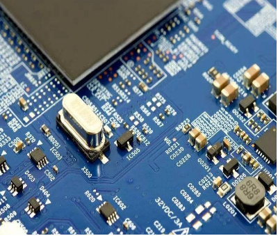
PCB制造

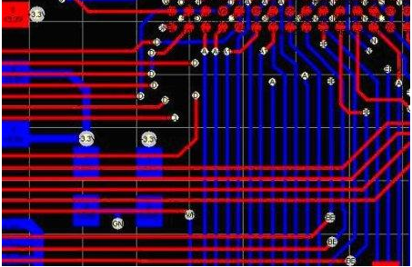
Consideration of PCB Proofing Pad Aperture Size
When insert component pads, the pad size shall be appropriate. If the pad is too large, the solder spreading area will be large, and the solder joints formed will not be full, while if the surface tension of copper foil of SMAller pad is too small, the solder joints formed will not soak the solder joints. The fit clearance between the hole diameter and the component line is too large, whICh is easy to solder. When the hole diameter is 0.05~0.2mm wider than the lead wire and 2~2.5 tiMES the pad diameter, it is an ideal condition for welding.
The PCB proofing is carried out according to the requirements of the pad to achieve the minimum diameter, which is at least 0.5mm larger than the maximum diameter of the keyhole flange of the welding terminal. Test pads must be provided for all nodes in accordance with ANSI/IPC2221. Node refers to the electrical connection point between two or more components. A test pad requires a signal name (node signal name), x-y coordinate axis related to the reference point of the PCB, and the coordinate position of the test pad (indicating which side of the PCB the test pad is located on).
Consideration of PCB Proofing Pad Aperture Size
The aspect ratio of plated through-hole has an important influence on the ability of pcb proofing manufacturers to conduct effective electroplating in plated through-hole, and is also important to ensure the reliability of the PTH/PTV structure. When the hole size is less than 1/4 of the basic circuit board thickness, the tolerance shall be increased by 0.05mm. When the hole diameter is 0.35mm or smaller, and the aspect ratio is 4:1 or larger, the pcb proofing manufacturer should cover or block the plated through hole in a suitable way to prevent the entry of solder. In general, the ratio of PCB thickness to plated through-hole spacing should be less than 5:1. It is necessary to provide the SMT with the information of the fixed devices, and also need the temperature closing technology of the printed circuit board assembly layout to promote the testability in the circuit with the help of the "fixed device for testing in the circuit" or commonly referred to as the "nail bed fixed device".
PCB proofing
To achieve this goal, we need to do the following:
1. Avoid plating through holes - probe on both sides of the printed circuit board. Place the test tip through the hole on the non component/welding surface of the printed circuit board. In this way, reliable and cheaper devices can be used. The number of different hole sizes should be kept to a minimum.
2. The diameter of the test pad specially used for detection shall not be less than 0.9mm.
3. Do not rely on the edge of the connector pointer for pad testing. The test probe can easily damage the gold plated pointer.
4. The space around the PCB pad shall be greater than 0.6mm and less than 5mm. If the height of the component is greater than 6.7mm, the test pad shall be placed 5mm away from the PCB component.
5. Do not place any components or test pads within 3mm from the edge of the printed circuit board.
6. The test PCB pad shall be placed in the center of a 2.5mm hole in a grid. Where possible, standard probes and a more reliable fixture are permitted.


抖音二維碼

Q Q二維碼

微信二維碼
點擊
然后
聯(lián)系
然后
聯(lián)系
電話熱線
13410863085Q Q

微信

- 郵箱