鑫景福致力于滿足“快速服務,零缺陷,輔助研發”PCBA訂購單需求。


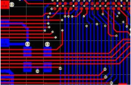
PCB制造
In PCB proofing, a lead tin anti-corrosive layer is pre coated on the copper foil part to be reserved on the outer layer of the board, that is, the graphIC part of the circuit, and then the rest of the copper foil is chEMIcally etched, which is calLED etching.
As the last step of PCB from optical board to displaying circuit graphics, what quality problems should be paid attention to in etching?
The quality requirement of etching is to completely remove all copper layers except under the corrosion resistant layer. Strictly speaking, the etching quality must include the consistency of wire width and the degree of side etching.
Side etching is often discussed in etching. The ratio of side etching width to etching depth is called etching factor; In the printed PCB circuit industry, SMAll side etching degree or low etching factor is the most satisfactory. The structure of the etching equipment and the etching solution with different components will affect the etching factor or side etching degree.
In many ways, the quality of etching existed long before the PCB entered the etching machine. Because there is a very close internal relationship between each process of PCB proofing, there is no process that is not affected by other processes and does not affect other processes. Many problems identified as etching quality have actually existed in PCB processes prior to film removal or even earlier.
PCB proofing
Theoretically, PCB proofing enters the etching stage. In the pattern electroplating method, the ideal state should be: the total thickness of copper and lead tin after electroplating should not exceed the thickness of the electroplating sensitive film, so that the electroplating pattern is completely blocked by the "walls" on both sides of the film and embedded in it. However, in real production, the coating pattern is much thicker than the photosensitive pattern; As the coating height exceeds the photosensitive film, there is a trend of horizontal accumulation. The tin or lead tin anti-corrosive layer covered above the line extends to both sides, forming a "edge", covering a small part of the photosensitive film below the "edge". The "edge" formed by tin or lead tin makes it impossible to completely remove the photographic film when removing the film, leaving a small part of "glue residue" below the "edge", resulting in incomplete etching. The "copper root" is formed on both sides of the line after etching, which narrows the line spacing, causing the printed PCB board to fail to meet customer requirements and may even be rejected. Rejection will greatly increase the production cost of PCB.
In PCB proofing, once problems occur in the etching process, it is bound to be a batch problem, which will eventually cause great potential quality problems for products. Therefore, it is particularly important to find a suitable PCB proofing manufacturer. We are committed to solving the pain point that enterprises have no place to process difficult, precise and special boards in PCB proofing. In every link of PCB proofing, PCB technology can be well controlled to deliver high-quality PCB proofing products to customers.


抖音二維碼

Q Q二維碼

微信二維碼
點擊
然后
聯系
然后
聯系
電話熱線
13410863085Q Q

微信

- 郵箱