鑫景福致力于滿足“快速服務(wù),零缺陷,輔助研發(fā)”PCBA訂購單需求。


PCB制造
We first know PCB. PCB is a printed circuit board, whICh is the basis and carrier of electronIC components and related electrical links. It is generally calLED PCB bare board, while PCBA is a process of welding on PCB through SMT chip/AI (automatic plug-in) and other process technologies based on PCB bare board. Examples of PCB and PCBA are as follows:
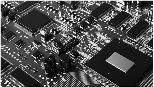
PCB
PCB
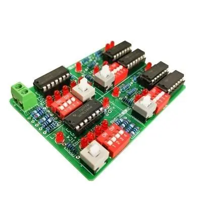
PCBA
It can be clearly seen that PCBA is a process formed by combining SMT and AI technologies on PCB. Strictly speaking, PCBA=PCB+components+SMT/AI+firmware+test.
Now let's take a look at the general steps of PCBA production:
SMT refers to Surface Mount Technology, which is the process of mounting electronic components on the surface of pcb and soldering through reflow soldering. SMT can also be divided into the following steps:
Solder paste printing
Place the unfrozen solder paste on the steel MESh, and print the tin evenly on the PCB through the scraper. The common solder paste is lead-free solder paste, and usually cooperate with the solder paste detector to detect the thickness and printing effect of the solder paste.
Hands on chip
Install the components on the feeder, use the nozzle to suck the components from the mounting head, and place the components on the PCB pad according to the specified procedure.
Reflow soldering
Through high temperature heating and melting of solder paste, the components and PCB pads can be tightly combined, and the components can be firmly welded to the board. For the boards that have been reflowed, AOI (automatic optical detection) can be used to detect the PCB welding effect, which can detect the missing parts/displacement/monument/direction, tin connection and other abnormalities.
plug-in unit
Insert the components packaged by DIP into the corresponding positions of PCB, and then conduct wave soldering to fix the pins on the bonding pad, cut off the redundant pins, and clean the traces of wave soldering.
Firmware burning
Use the burner to burn the firmware into the IC through the burning port. This step can also be completed before the IC is mounted. Use the burner to burn the firmware into the IC in batches.
test
Generally, it is divided into basic function test, environmental resistance test, EMC test, mechanical stress impact test and PCBA test, which are very critical process flows. Testing directly affects the quality of products. Different product requirements have different testing processes and means.
Apply three proofing paint
The three proofing paint is a special coating, which is sprayed on PCBA board to achieve the purpose of moisture-proof, salt fog proof and corrosion prevention. It can protect against the harmful environment, and can also well prolong the service life of the product.


抖音二維碼

Q Q二維碼

微信二維碼
點擊
然后
聯(lián)系
然后
聯(lián)系
電話熱線
13410863085Q Q

微信

- 郵箱