鑫景福致力于滿足“快速服務(wù),零缺陷,輔助研發(fā)”PCBA訂購單需求。


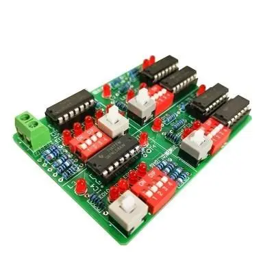
PCB制造
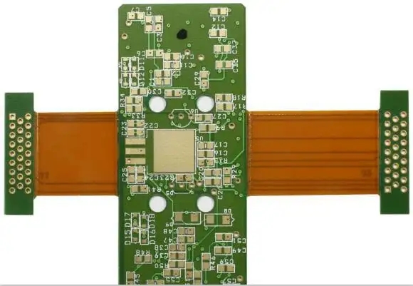
Rigid and flexible printed circuit boards are manufactured through PCB manufacturing process combining rigid and flexible circuit boards. The two boards are then permanently interconnected to form various types of PCBs. In the manufacturing process of rigid and Flexible circuit boards, some factors and precision must be considered to produce a perfect final product.
Some more important considerations are:
L Laser contour cutting
L Selective pad electroplating
L Material dimensional tolerance
L Thin material handling capacity and procedures, and
L PlaSMA decontamination and corrosion back
Compared with traditional rigid PCBs, flexible substrate materials for manufacturing rigid PCB have more advantages. They are:
L Lighter weight
L can be used to interconnect components,
L Less thICkness
L Dynamic bending
L Save more space,
L Excellent electrical and thermal performance,
L To give just a few examples, it has a high degree of freedom in electronIC design and mechanical design.
Flexible circuit board
Steps involved in the rigid Flex design and manufacturing process
1. Preparation of basic PCB materials:
The first step in the rigid Flexible manufacturing process is to prepare/clean the laminate. The laminate consists of a copper layer (with an adhesive coating) that must be thoroughly cleaned before proceeding to the next step. Basically, the purpose of pre cleaning is to remove the rust preventive coating used by the supplier to coat the copper coil to prevent oxidation. To remove the coating, the manufacturer performs the following steps:
L First, immerse the copper coil in concentrated acid solution.
L Sodium persulfate treatment is used for micro etching copper coils.
L The copper coil shall be fully coated with a suitable oxidant to provide adhesion and oxidation protection
2. Circuit pattern generation
After preparing the basic materials, the next step is to generate circuit patterns. This is done using two main techniques:
L Screen printing: This is the most popular PCB technology. It creates the desired pattern directly on the surface of the laminated pcb board. The maximum total thickness is 4-50 microns.
L Photographic imaging: This technology is the oldest technology and is usually used to depict the circuit routing on the laminate. The pattern is transferred from the photomask to the laminate using a dry photoresist film and ultraviolet light.
3. Etch the circuit pattern
After generating the desired pattern, the copper laminate is then carefully etched. This process can be performed by immersing the laminate in an etching bath or exposing it to an etchant spray. In order to obtain perfect results, both sides of the laminate must be etched at the same time.
4. Drilling process
High speed tools with 100% accuracy can be used to manufacture a large number of holes, pads and through holes. Laser drilling technology is used for ultra small holes.
5. Through hole electroplating
This process is very precise and cautious. The drilLED holes are accurately deposited with copper and electroless plated to form an electrical interconnection layer.
6. Apply the covering layer or covering layer.
An overlay is applied to protect the top and bottom sides of the rigid flexible circuit board. Its main purpose is to provide comprehensive protection for the circuit board from the adverse physical and chEMIcal conditions. Polyimide film is usually used, and screen printing technology is used to imprint it on the surface.
7. Cut out Flex
Carefully cut and blank individual flex plates. For batch production, hydraulic drilling is used, while special knives are used in small batch production.
8. Electrical testing and verification.
Testing and verification is the last and final step. The integrity of rigid flexible circuit boards must be evaluated, because even the slightest defect will seriously affect the function, performance and durability of the final rigid flexible circuit boards.


抖音二維碼

Q Q二維碼

微信二維碼
點(diǎn)擊
然后
聯(lián)系
然后
聯(lián)系
電話熱線
13410863085Q Q

微信

- 郵箱