鑫景福致力于滿足“快速服務,零缺陷,輔助研發”PCBA訂購單需求。


PCB制造
ElectronIC factory editor: detaiLED explanation of pcb proofing stack number
A good stack structure is the best preventive measure against most signal integrity problems and EMC problems, and it is also the most easily misunderstood. There are several factors at work. A good solution to one problem may lead to the deterioration of other problems. Many system design suppliers recommend that there should be at least one continuous plane in the circuit board to control the characteristic impedance and signal quality. As long as the cost is affordable, this is a good suggestion. EMC consulting experts often recommend placing ground fill or ground layer on the outer layer to control electromagnetic radiation and sensitivity to electromagnetic interference, which is also a good suggestion under certain conditions.
However, due to the transient current, this method may encounter difficulties in some common designs. First, let's look at a SIMple case of a pair of power/ground layers: it can be seen as a capacitor. It can be considered that the power layer and the ground layer are two electrodes of the capacitor. In order to obtain a larger capacitance value, it is necessary to close the two plates closer (D) and increase the dielectric constant( ε r)。 The larger the capacitance, the lower the impedance, which is what we hope, because it can suppress noise. No matter how other layers are arranged, the main power layer and ground layer shall be adjacent and in the middle of the stack. If the distance between the power layer and the ground layer is large, it will cause a large current loop and bring a lot of noise. For an 8-layer board, placing the power layer on one side and the ground layer on the other side will cause the following problems:
1. Maximum crosstalk. As the mutual capacitance increases, the crosstalk between signal layers is greater than that of each layer itself.
2. Maximum circulation. The current flows around each power layer in parallel with the signal, and a large amount of current enters the main power layer and returns through the ground layer. EMC characteristics will deteriorate due to the increase of circulation.
3. Loss of control over impedance. The farther the signal is from the control layer, the lower the accuracy of impedance control is because there are other conductors around.
4. It is easy to cause solder short circuit, which may increase the cost of the product.
We must make a compromise between performance and cost. For this reason, I would like to share my views on how to arrange digital circuit boards to obtain the best SI and EMC features.
The distribution of PCB layers is generally symmetrical. In my humble opinion, more than two signal layers should not be placed adjacent; Otherwise, the control of SI will be lost to a large extent. It is better to place the internal signal layers symmetrically in pairs. Unless some signals need to be connected to SMT devices, we should minimize the outer signal wiring.
For circuit boards with more layers, we can repeat this placement method for many tiMES (Figure 2). Additional power and ground layers can also be added; Just ensure that there is no paired signal layer between the two power layers.
The wiring of high-speed signal shall be arranged in the same pair of signal layers; Unless this principle has to be violated due to the connection of SMT devices. All routing of a signal shall have a common return path (i.e. ground layer). There are two ideas and methods to judge which two layers can be regarded as a pair:
1. Ensure that the return signals at equal distances are completely equal. This means that the signals should be symmetrically routed on both sides of the internal ground plane. The advantage of this is that it is easy to control the impedance and circulation; The disadvantage is that there are many vias on the ground wire layer, and there are some useless layers.
2. Two signal layers of adjacent wiring. The advantage is that the vias in the ground wire layer can be controlled to the minimum (using embedded vias); The disadvantage is that the effectiveness of this method decreases for some key signals.
I prefer the second method. The grounding connection of the component driving and receiving signals should preferably be connected directly to the layer adjacent to the signal wiring layer. As a simple wiring principle, the surface wiring width measured in inches should be less than one-third of the rise time of the driver measured in inches (for example, the wiring width of high-speed TTL is 1 inch).
If the power is supplied by multiple power sources, a ground wire layer must be laid between each power supply metal wire to separate them. Capacitance shall not be formed to avoid AC coupling between power supplies.
The above measures are to reduce circulating current and crosstalk, and enhance impedance control capability. The ground layer also forms an effective EMC "shielding box". Under the prEMIse of considering the influence on the characteristic impedance, the ground wire layer can be made of any surface area that is not used.
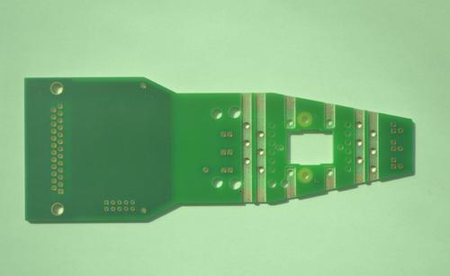
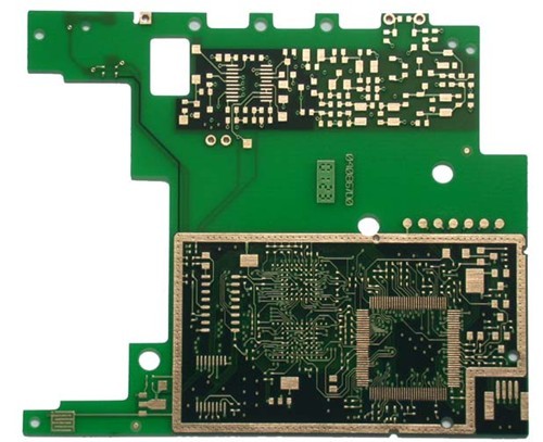
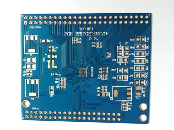
PCB manufacturers, PCB designers and PCBA manufacturers will explain the problem of the number of layers of PCB proofing.


抖音二維碼

Q Q二維碼

微信二維碼
點擊
然后
聯系
然后
聯系
電話熱線
13410863085Q Q

微信

- 郵箱