鑫景福致力于滿足“快速服務,零缺陷,輔助研發”PCBA訂購單需求。


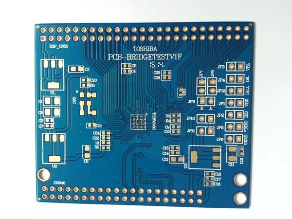
PCB制造
DetaiLED explanation of pcb proofing characteristic impedance and EMC
Pcb proof characteristIC impedance
A good stack structure can effectively control the impedance, and its routing can form an understandable and predictable transmission line structure. The field solution tool can deal with this kind of problem very well. As long as the number of variables is controlled to the minimum, a fairly accurate result can be obtained.
However, when more than three signals are stacked together, this is not necessarily the case. The reason is very subtle. The target impedance value depends on the process technology of the device. High speed CMOS technology can generally reach about 70 Ω; High speed TTL devices can generally reach about 80 Ω to 100 Ω. Because the impedance value usually has a great impact on noise tolerance and signal switching, it is necessary to be very careful when selecting impedance; The product manual should give guidance on this.
The initial results of the field resolution tool may encounter two problems. First of all, the field of vision is limited. The on-site solution tool only analyzes the impact of nearby routing, and does not consider the non parallel routing on other layers that affect impedance. The field solution tool cannot know the details before wiring, that is, when allocating the wiring width, but the above paired arrangement method can minimize this problem.
It is worth mentioning the impact of partial power planes. The outer circuit board is often crowded with grounding copper wires after wiring, which is conducive to EMI suppression and balance placing. If only such measures are taken for the outer layer, the laminated structure recommended in this paper will have very little impact on the characteristic impedance.
The effect of using a large number of adjacent signal layers is very significant. Some on-site solution tools cannot find the existence of copper foil, because they can only check the printed wire and the whole layer, so the analysis result of impedance is incorrect. When there is metal on the adjacent layer, it is like an unreliable ground wire layer. If the impedance is too low, the instantaneous current will be large, which is a practical and sensitive EMI problem.
Another cause of impedance analysis tool failure is distributed capacitance. These analysis tools generally can not reflect the influence of pins and vias (this influence is usually analyzed by emulators). This effect can be significant, especially on the backplane. The reason is very SIMple:
The characteristic impedance of PCB proofing can generally be calculated by the following formula: √ L/C
Where L and C are inductance and capacitance per unit length, respectively.
If the pins are evenly arranged, the additional capacitance will greatly affect the calculation result. The formula will become:
√L/(C+C')
C 'is the pin capacitance per unit length.
If the connectors are connected in a straight line as on the backplane, the total line capacitance and the total pin capacitance except the first and last pins can be used. In this way, the effective impedance will be reduced, even from 80 Ω to 8 Ω. To obtain the effective value, divide the original impedance value by:
√(1+C'/C)
This calculation is important for component selection.
The capacitance of components and packages (and sometiMES inductance) should be taken into account during delay simulation. Two problems should be noted. First, the simulator may not be able to correctly simulate distributed capacitors; Secondly, we should also pay attention to the impact of different production conditions on the incomplete level and non parallel routing. Many field solution tools cannot analyze the stack distribution without full power or ground layers. However, if the signal layer is adjacent to a ground wire layer, the calculated delay will be very bad. For example, the capacitance will have the maximum delay; If both layers of a double-sided board are covered with many ground wires and VCC copper foils, this situation is more serious. If the process is not automated, it will be very messy to set these things in a CAD system.
PCB proofing EMC
EMC has many influencing factors, many of which are usually not analyzed. Even if they are analyzed, it is often too late after the design is completed. Here are some factors that affect EMC:
The slot in the power layer will form a quarter wavelength antenna. Drilling method shall be used to replace the occasion where the installation slot is required on the metal container.
Inductive element. I once met a designer who followed all the design rules and made simulations, but his circuit board still had a lot of radiation signals. The reason is that two inductors on the top layer are placed in parallel with each other, forming a transformer.
Due to the influence of incomplete ground plane, the low impedance of the inner layer causes large transient current of the outer layer.
Using defensive design can avoid most of these problems. First of all, we should make the correct stack structure and routing strategy, so that we have a good start.
PCB manufacturers, PCB designers and PCBA manufacturers will explain the characteristic impedance of pcb proofing and EMC details.


抖音二維碼

Q Q二維碼

微信二維碼
點擊
然后
聯系
然后
聯系
電話熱線
13410863085Q Q

微信

- 郵箱