鑫景福致力于滿足“快速服務(wù),零缺陷,輔助研發(fā)”PCBA訂購單需求。


PCB制造

What is the PCB for pcb proofing and component installation
For PCB proofing, we need to make an electronIC product, usually we first design the circuit schematic diagram On the circuit schematic diagram, various specific symbols are used to represent different electronIC components and connect them with wires An electronic engineer can clearly see the working principle of the circuit and the functions of each part through these symbols and connections If the circuit design is correct, you only need to prepare the required electronic components, and then connect them with wires to work Most of the early electronic products are like this. If you have a tube radio in the 1960s and 1970s, you can see the MESsy components and crisscross wires
Fortunately, the circuit of the tube radio is relatively SIMple, but if you want to build a more complex product, such as a computer motherboard, you can think about the results if you still use the above methods It may take tens of thousands of wires, and then weld them one by one. I'm afraid the most skilLED workers will be tired. In addition, mass production cannot be carried out with this method. Therefore, we need PCBs
What is PCB
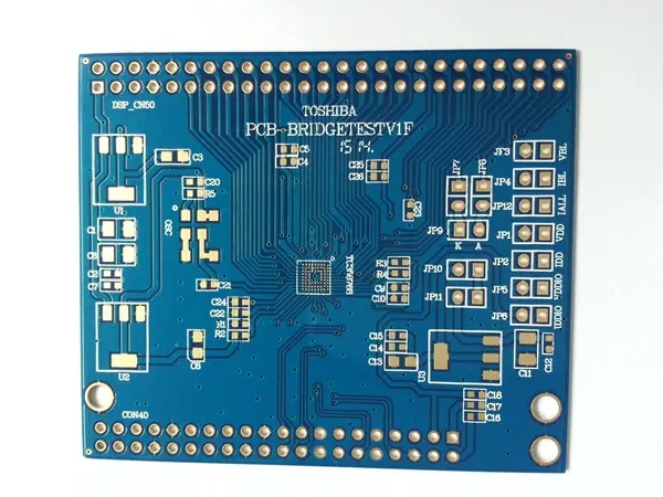
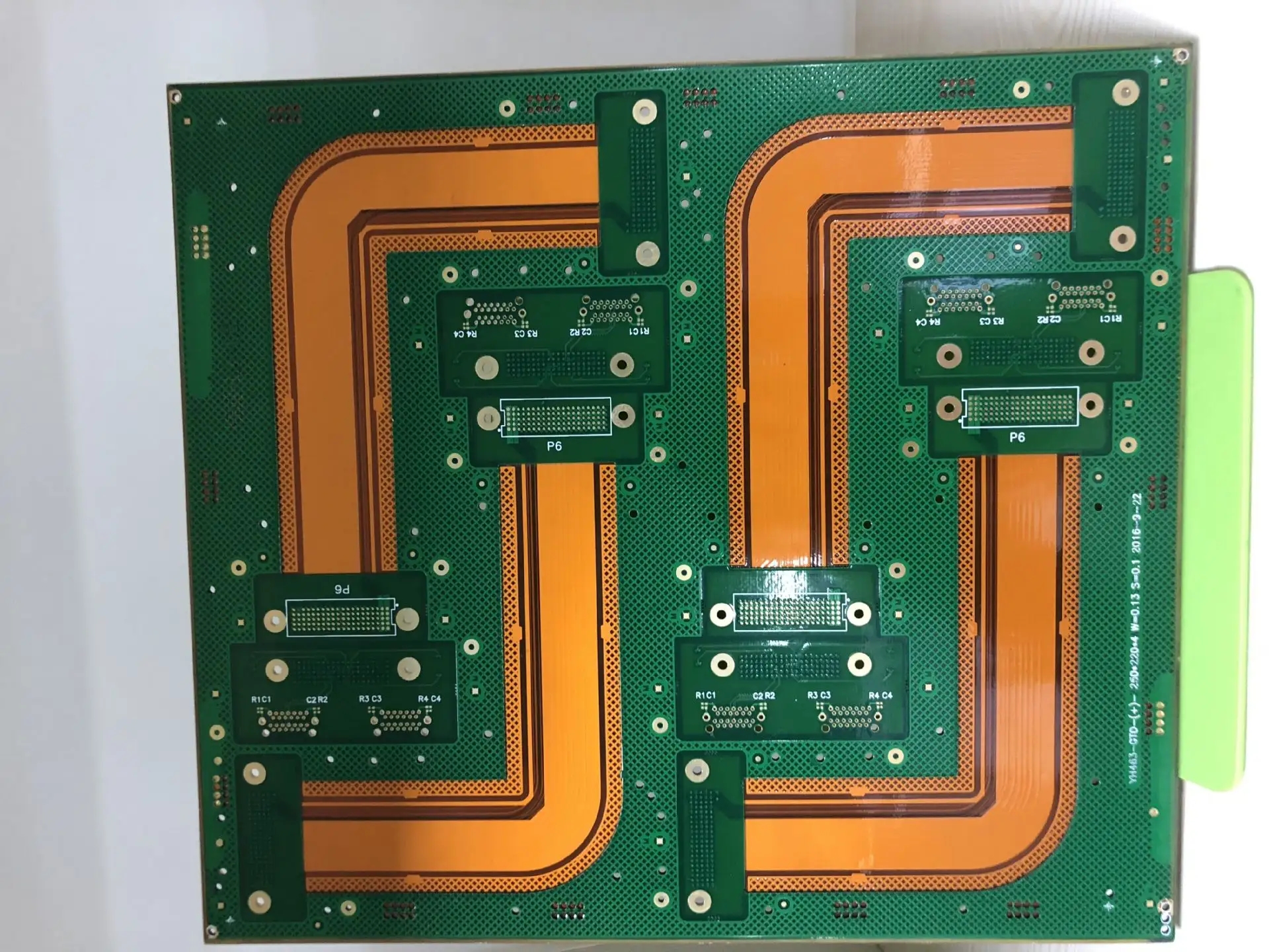
PCB is the abbreviation of "Printed Circuit Board", which literally means printed circuit board Its meaning is: a board with a certain size processed from insulating material as the base plate and at least one conductive pattern and designed hole on it to realize the electrical connection between electronic components. Such a board is called a printed circuit board
Generally speaking, PCB is obtained by etching copper clad plate The copper clad plate is composed of a plate base and copper foil. The plate base is usually made of insulating materials such as glass fiber, which is covered with a layer of copper foil (usually oxygen free copper) After etching, the copper foil is left with sections of zigzag copper foil. These copper foils are called traces These wiring functions are equivalent to those in the circuit schematic diagram. They are responsible for connecting the pins of components together. There are holes drilled in the copper foil for installing electronic components, which are called drilling holes. The copper foil used for welding with component pins is called pad
Obviously, PCB can provide fixed and assembled mechanical support for electronic components and can realize electrical connection or insulation between electronic components In addition, we can see that many PCBs are printed with component numbers and some graphics, which facilitates component insertion, inspection and maintenance
How can components be installed on PCB
Since we have mentioned that PCB can provide mechanical support and electrical connection for electronic components, how are these electronic components installed on PCB? In fact, electronic components have many packaging forms, and different packaging forms of components have different installation methods on PCB Traditional electronic components are mostly pin type and large in size. For such components, they can only be installed after drilling holes on PCB The component pins pass through the drill hole and are welded on the pad on the other side of the PCB. After welding, cut off the redundant pins However, nowadays, computer boards and cards mostly use SMD surface mount components with low cost and SMAll volume, so it is unnecessary to drill holes on PCB, as long as the components are stuck on the designed position and welded on the bonding pad. In addition to being directly welded to PCB, components can also be installed through sockets For example, most of the well-known BIOS chips are installed on the motherboard with sockets
The concepts of element face and welding face are often mentioned in some materials The component surface is the side where the electronic components are located, and the welding surface is the side where the component pins are connected with the bonding pad on the PCB through soldering tin. It is used for welding For pin type components, solder joints and components are located on two surfaces of PCB respectively, and components can only be located on the component surface, otherwise it will bring huge trouble to welding For SMD components, the solder joints and components are on the same surface, so the components can be on any surface or even two surfaces of the PCB
PCB manufacturers, PCB designers and PCBA manufacturers will explain to you what PCB samples are and component installation.


抖音二維碼

Q Q二維碼

微信二維碼
點擊
然后
聯(lián)系
然后
聯(lián)系
電話熱線
13410863085Q Q

微信

- 郵箱