鑫景福致力于滿足“快速服務,零缺陷,輔助研發”PCBA訂購單需求。


PCB制造
DetaiLED explanation of PCB noise reduction processing method
When we design the circuit board, the circuit principle design is very good, or even excellent. However, during the debugging process, there will be a variety of noises, and the circuit board can not achieve the desired purpose. SometiMES even worse, we have to play the board again. So how can we reduce the noise of the circuit board? Let's analyze it.
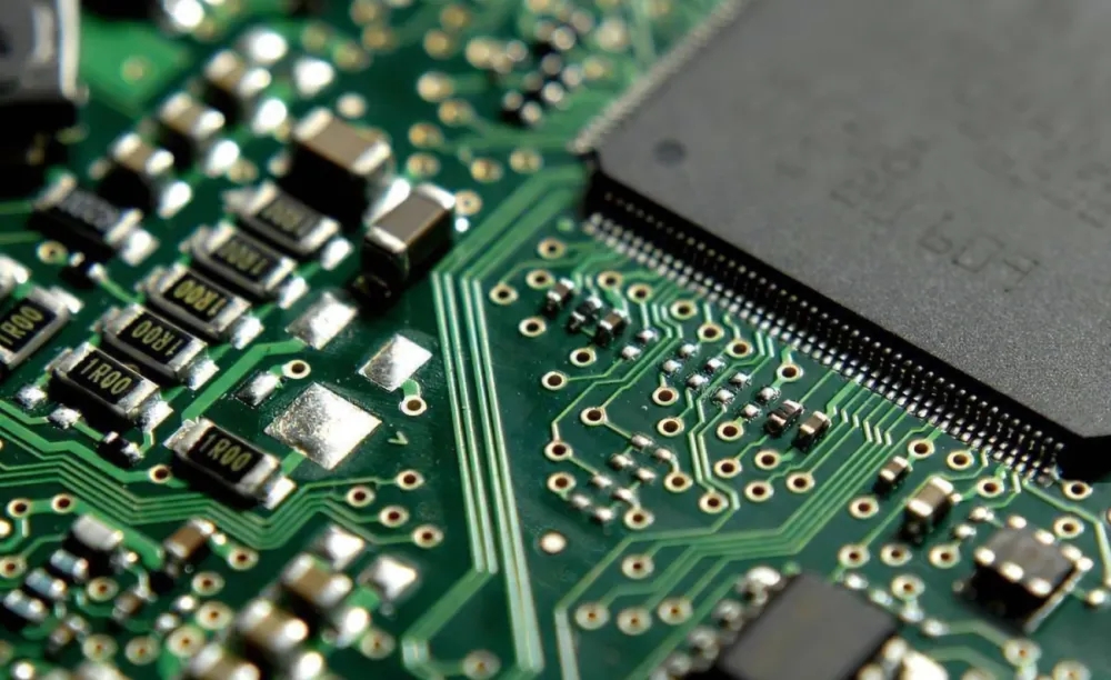
We electronIC engineers can see the general distribution of a board with good performance at a glance (provided that we know what the function of the board is), which is the principle of functional module separation. A functional module is a collection of circuits in which some electronIC components are combined to complete a certain function. In actual design, we need to close these electronic components and reduce the wiring length between electronic components in order to increase the role of circuit modules. In fact, it is not difficult to understand that our common development boards or mobile phones do this, especially for mobile phones. If you take the mobile phone apart, you will find that the separation between modules is obvious, and each module is shielded with Faraday cages.
Secondly, it should be noted that when there are analog and digital circuits on a PCB, they need to be separated. If you have to make a hat, there is a silent zone. The so-called silent area is the area where analog circuits and digital circuits or various functional modules are physically isolated. In this way, it can prevent other modules from interfering with the module. In the cell phone circuit board mentioned above, the silent zone is obvious. Note that the quiet area is not connected to the ground of the circuit board.
In the actual circuit design, not every PCB board has enough space for us to do the silent area. So, how do we design when space is not allowed?
A. Use transformer or signal isolation element for design. This is the meaning of circuit separation that we often use CMOS or crystal triode and other components.
B. The signal passes through the filter circuit before entering the module. This method is a common method to prevent ESD. It is also considered that this method can eliminate noise (ESD, high-frequency and high-voltage noise).
C. Common mode inductors are used for signal protection. If we do not know the function of the common mode inductor, we will find that there are only two coils in the schematic diagram, which has no effect. In fact, it is not. It plays an important role in signal stability and noise elimination. This also reveals that electronic engineers need a long time of training to grow.
A method SIMilar to the silent zone design of circuit boards is ditch protection technology. This technology is to remove the divided copper skin of the silent area to form a bare circuit board material. And the concept of bridge is also extended from this: the power supply, ground and signal lines connecting each sub area together are called bridges. Trench protection technology has the ability to withstand the impact of peak voltage and classical discharge protection, and plays a role in reducing circuit board noise to a certain extent. In the circuit board design, RF loop current will be generated when wiring irrelevant to the isolation area passes through the trench, which will further affect the performance of the circuit board. This should be noted.
Now, many analog to digital or digital to analog components have connected two parts of the ground inside the component, typically ADC and DAC devices. These devices should have a standard reference ground for segmentation. If the digital signal current cannot effectively return to the source, it will cause noise and generate EMI. When drawing the schematic diagram, we found that AGND and DGND pins are a device with superior performance, It will reduce the difficulty of our design.
In general, the circuit is partitioned according to modules, and obvious quiet zones are set between partitions to minimize the impact of power and ground on signals and minimize the noise of the circuit board.
PCB manufacturers, PCB designers, and PCBA manufacturers will explain how to reduce PCB noise.


抖音二維碼

Q Q二維碼

微信二維碼
點擊
然后
聯系
然后
聯系
電話熱線
13410863085Q Q

微信

- 郵箱