鑫景福致力于滿足“快速服務,零缺陷,輔助研發”PCBA訂購單需求。


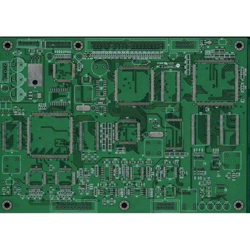
PCB制造
Introduction to PCB classifICation, working principle and composition
Printed Circuit Board, literally translated as "printed circuit board", also known as circuit board, PCB, PCB, etc., is an indispensable part of electronic equipment in today's scientific and technological era. The emergence of circuit board makes it possible for many functions of electronic products and circuit integration. It is mainly composed of pads, vias, mounting holes, wires, components, connectors, filling, electrical boundaries, etc. The main functions of each component are as follows:
Soldering pad: metal hole for soldering component pins.
Through hole: It can be divided into metal through hole and non-metal through hole. The metal through hole is used to connect the component pins between layers.
Mounting hole: fix the circuit board.
Conductor: copper film of electrical network connecting the pins of components.
Connector: component connected between circuit boards.
Filling: copper coating of ground wire network can effectively reduce impedance.
Electrical boundary: determine the size of the circuit board, and all components on the circuit board shall not exceed the boundary.
Circuit board classification:
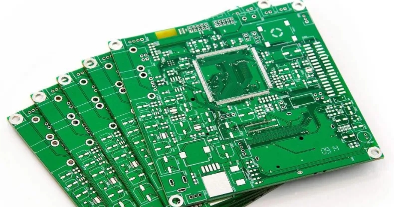
According to the number of layers, PCB can be divided into three major categories: single panel, double panel, and multi-layer PCB. Single panel: on the most basic PCB, parts are concentrated on one side and wires are concentrated on the other side. Because the wire only appears on one side, this PCB is calLED single-sided circuit board. Double panel is an extension of single panel. When single layer wiring cannot meet the needs of electronic products, double panel may be used. Both sides are copper coated and wired, and the line between the two layers can be conducted through the via to form the required network connection. Multilayer board refers to a printed board with more than three conductive graphic layers and insulating materials between them laminated at intervals, and the conductive graphics between them are interconnected as required. multilayer circuit board (MLPCB) is the product of the development of electronic information technology in the direction of high speed, multi-function, large capacity, SMAll volume, thin and lightweight.
Understand the working principle and composition of the circuit board in detail
The circuit board can be called a printed circuit board or a printed circuit board, and its English name is (Printed Circuit Board) PCB (Flexible Printed Circuit board) FPC circuit board FPC circuit board, also known as Flexible circuit board, is a highly reliable and excellent flexible printed circuit board made of polyimide or polyester film. The naMES of circuit boards include: ceramic circuit board, alumina ceramic circuit board, aluminum nitride ceramic circuit board, circuit board, PCB, aluminum substrate, high-frequency board, thick copper plate, impedance board, PCB, ultra-thin circuit board, ultra-thin circuit board, printing (copper etching technology) Circuit board, etc.
working principle
The working principle of the circuit board is to use the board based insulating material to isolate the conductive layer of copper foil on the surface, so that the current flows in various components along the pre designed route to complete functions such as work, amplification, attenuation, modulation, demodulation, coding, etc.
form
The circuit board is mainly composed of bonding pads, vias, mounting holes, wires, components, connectors, thin film circuit SMT patch of Watford circuit board, thin film circuit SMT patch of Watford circuit board, filling, electrical boundary, etc. The main functions of each component are as follows:
Soldering pad: It is used to weld metal holes of component pins.
Through hole: there are metal through hole and non-metal through hole, in which the metal through hole is used to connect the component pins between layers.
Mounting hole: used to fix the circuit board.
Wire: copper film of electrical network used to connect the pins of components.
Connector: components used for connecting circuit boards.
Filling: copper coating for ground wire network can effectively reduce impedance.
Electrical boundary: used to determine the size of the circuit board. All components on the circuit board cannot exceed this boundary.
classification
According to the number of layers, PCB can be divided into single panel, double panel, and multi-layer PCB.
Multilayer board: refers to a printed board with more than three conductive graphic layers and insulating materials between them laminated at intervals, and the conductive graphics between them are interconnected as required. Multilayer circuit board (MLPCB) is the product of the development of electronic information technology in the direction of high speed, multi-function, large capacity, small volume, thin and lightweight.
Single panel: On the most basic PCB, parts are concentrated on one side and wires are concentrated on the other side. Because wires only appear on one side, this PCB is called single-sided circuit board. Single panel is usually SIMple to make and low in cost, but its disadvantage is that it cannot be applied to too complex products.
Double sided board: It is an extension of single panel. When single layer wiring cannot meet the needs of electronic products, it is necessary to use double sided boards. Both sides are copper coated and wired, and the line between the two layers can be conducted through the via to form the required network connection.
PCB can be divided into soft board (FPC), hard board (PCB) and soft hard combination board (FPCB) according to characteristics.
Working level
The circuit board includes many types of working layers, such as signal layer, protective layer, silk screen layer, internal layer, etc. The functions of various layers are briefly introduced as follows:
(1) Protective layer: mainly used to ensure that the parts on the circuit board that do not need tinning are not tinned, so as to ensure the reliability of the circuit board operation. Top Paste and Bottom Paste are the top layer and bottom layer respectively; Top Solder and Bottom Solder are respectively solder paste protective layer and bottom solder paste protective layer.
(2) Signal layer: mainly used for placing components or wiring. Protel DXP usually contains 30 middle layers, namely Mid Layer1~Mid Layer30. The middle layer is used to lay signal lines, and the top and bottom layers are used to place components or copper coating.
(3) Screen printing layer: mainly used to print the serial number, production number, company name, etc. of components on the circuit board.
(4) Internal layer: mainly used as the signal wiring layer. Protel DXP includes 16 internal layers.
(5) Other layers: mainly including 4 types of layers.
Drill Guide: mainly used for drilling position on PCB.
Keep Out Layer: mainly used to draw the electrical border of the circuit board.
Drill Drawing: mainly used to set the drilling shape.
Multi Layer: mainly used to set multi surface layer.
PCB manufacturers, PCB designers and PCBA manufacturers will explain PCB classification, working principles and composition.


抖音二維碼

Q Q二維碼

微信二維碼
點擊
然后
聯系
然后
聯系
電話熱線
13410863085Q Q

微信

- 郵箱