鑫景福致力于滿足“快速服務,零缺陷,輔助研發”PCBA訂購單需求。


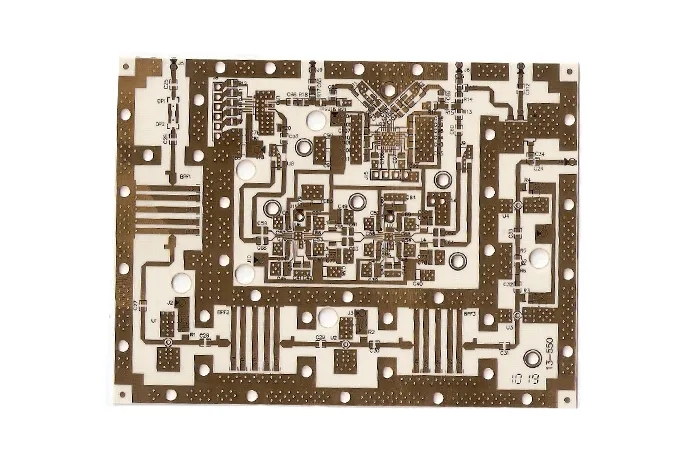
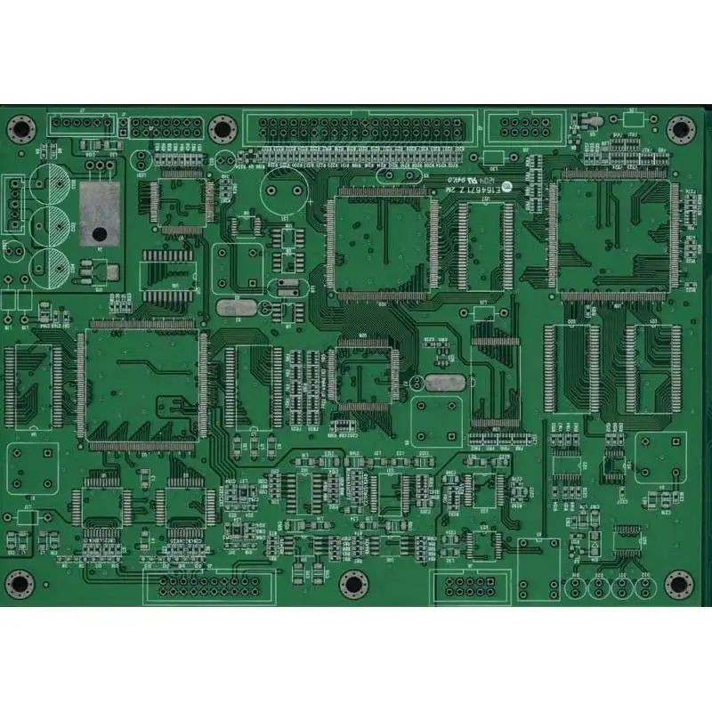
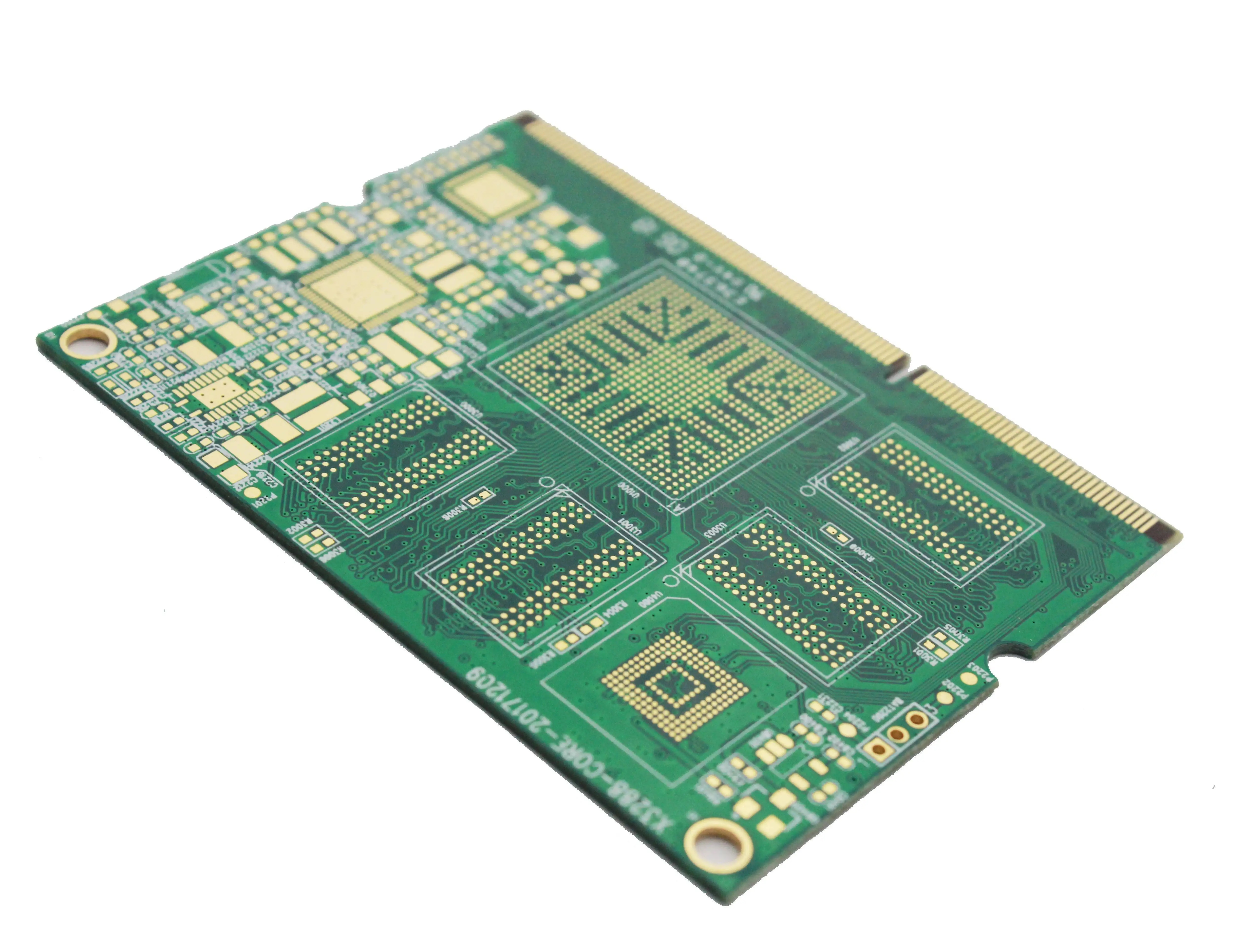
PCB制造
PCB copper chEMIcal precipitation, outer layer layout transfer and etching
PCB manufacturing, PCB design and PCBA processing manufacturers will explain PCB copper chemICal precipitation, outer layer layout transfer and etching
1. Chemical precipitation of copper on hole wall
Since almost all PCB designs use perforations to connect different layers of circuits, a good connection requires a 25 micron copper film on the hole wall. This thickness of copper film needs to be achieved by electroplating, but the hole wall is composed of non-conductive epoxy resin and glass fiber board.
So the first step is to deposit a layer of conductive material on the hole wall and form a 1 μ m copper film on the entire PCB surface, including the hole wall, by chemical deposition. The whole process, such as chemical treatment and cleaning, is controlLED by the machine.
Fixed PCB
Clean PCB
Shipping PCB
2. Transfer of outer PCB layout
Next, the outer layer PCB layout will be transferred to the copper foil. The process is SIMilar to the previous inner layer core board PCB layout transfer principle, which is to transfer the PCB layout to the copper foil using photocopied film and photosensitive film. The only difference is that the positive film will be used as the board.
The reduction method is used for the layout transfer of the inner layer PCB, and the negative film is used as the board. The PCB is covered by the cured photosensitive film. Clean the uncured photosensitive film. After the exposed copper foil is etched, the PCB layout circuit is protected by the cured photosensitive film and remains.
The normal method is adopted for the layout transfer of the outer layer PCB, and the positive sheet is used to make the board. The photoconductive film on the PCB is covered by a non circuit area. Clean the uncured photosensitive film and then conduct electroplating. Where there is a film, it cannot be plated. Where there is no film, copper is plated first and then tin is plated. After the film is removed, alkaline etching is carried out, and finally tin is removed. The circuit pattern remains on the board because it is protected by tin.
Clamp the PCB with a clip and plate the copper. As mentioned earlier, in order to ensure sufficient conductivity of the hole location, the copper film plated on the hole wall must have a thickness of 25 microns, so the entire system will be automatically controlled by the computer to ensure its accuracy.
3. Etching of outer PCB
Next, a complete automatic assembly line completes the etching process. First, clean the cured photosensitive film on the pcb board. Then wash the unwanted copper foil covered with it with strong alkali. Remove the tin coating on the copper foil of PCB layout with the tin remover. After cleaning, the 4-layer PCB layout is completed.
PCB is the most common and familiar device for hardware engineers. Through more accumulation and understanding of its characteristics, we can make it better used and develop more excellent innovative technology products.
PCB manufacturers, PCB designers and PCBA processors will explain PCB copper chemical precipitation, outer layer layout transfer and etching.


抖音二維碼

Q Q二維碼

微信二維碼
點擊
然后
聯系
然后
聯系
電話熱線
13410863085Q Q

微信

- 郵箱