鑫景福致力于滿足“快速服務,零缺陷,輔助研發”PCBA訂購單需求。


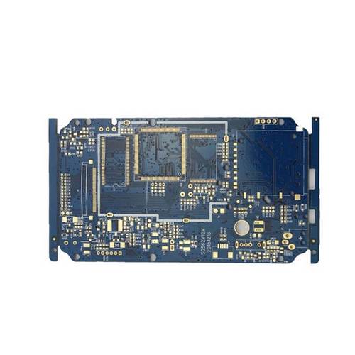
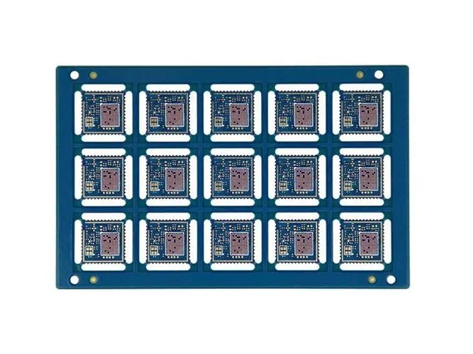
PCB制造
manufacturing process of thICk copper plate and causes of circuit board open circuit
Circuit board manufacturing, circuit board design and PCBA processing manufacturers explain the thick copper plate manufacturing process and the cause of circuit board open circuit
1. board selection
It is recommended to select high Tg sheet
For thick copper PCB, its thermal conductivity is strong due to the thick copper. When mounting under the same conditions, ordinary Tg plates are more prone to delamination bursting, white spots and other problems than high Tg plates.
2. Drilling
For thick copper PCB, due to the thick copper and the superposition of each layer, the copper is already in a large thickness. During drilling, the long time friction of the drill tool in the board is likely to cause wear or breakage of the drill tool, which will further affect the quality of the hole wall and further affect the reliability of the product.
3. Line
For thick copper printed circuit board, due to the thick copper, it is more difficult to process than ordinary board when etching the circuit. Therefore, increasing the line width spacing in the design is helpful to reduce the difficulty of etching processing, and also has a great improvement in the aspect of laminating and glue filling.
4. Pressing
For thick copper PCB, the thicker the copper is, the deeper the line gap is. In the case of the same copper residue rate, the required resin filling amount will increase, and multiple pieces of prepreg (PP) are required to meet the requirements of glue filling. When there are few resins, it is easy to cause glue deficiency, delamination and poor plate thickness uniformity;
Due to the superposition effect of the inner circuit and the limitation of resin flow, the thick copper circuit board will be thicker in the area with high copper residue rate than in the area with low copper residue rate after lamination, resulting in uneven thickness of the circuit board. Therefore, the uniformity of inner layer copper paving shall be improved as much as possible during design.
5. resistance welding
For thick copper PCB, due to the thick copper, it is easy to have problems such as substandard ink thickness, vertical flow, false copper exposure and bubbles when making solder mask. In the industry, it is usually realized by two solder mask printing and two exposure. Our company now has electrostatic spraying equipment to support better effect.
Reasons and solutions for circuit board open circuit
Causes and Treatment of Open Circuit on PCB
How to improve? Open circuit and short circuit of PCB circuit board are problems that manufacturers of multilayer pcb circuit board will encounter almost every day. These problems have been puzzling production and quality management personnel. Problems caused by insufficient quantity of goods (such as replenishment, delayed delivery and customer complaints) are relatively difficult to solve. I have more than 10 years of experience in PCB manufacturing, mainly engaged in production management, quality management, process management and cost control. We have accumulated some experience in improving the open circuit and short circuit of PCB. Now we have written a summary of the discussion on circuit board manufacturing. I hope it can be used for reference by colleagues engaged in production and quality management.
First, the main reasons for the open circuit of some PCB boards are summarized as follows:
The causes and improvement methods of the above phenomena are as follows:
Exposed substrate:
1. There are scratches on the copper clad laminate before it is stored.
2. The copper clad plate was scratched during blanking.
3. The copper clad laminate was scratched during transportation.
4. The copper foil on the surface of the production circuit board is scratched when passing through the horizontal machine.
5. The copper clad plate was scratched by the drill during drilling.
6. When copper foil is stacked after sinking, the surface is damaged due to improper operation.
Improvement method:
IQC must conduct spot check before entering the warehouse to check whether there is scratch on the surface of copper clad plate. If yes, contact the supplier in time and handle according to the actual situation.
2. Scratches caused by improper sinking or stacking of copper plates after electroplating: when the plates are stacked together after sinking and electroplating, the weight is not SMAll. When laying the board, the angle of the board is downward and there is a gravitational acceleration, which forms a strong impact force on the board surface and scratches on the board surface, exposing the base material.
3. The metal plate is scratched during transportation: when moving, the transmission lifts too many plates at a time, and the weight is too large. When moving, the plate is not lifted, but dragged along with the trend, causing friction between the corner and the plate surface, and scraping the plate surface. When the board is put down, the surface of the PCB board is scratched due to the friction between the circuit boards.
4. The copper clad plate was scratched during tapping. The main reason is that there are hard and sharp objects on the surface of the tapping machine workbench. When struck, the copper clad plate and sharp objects are scratched to form an exposed substrate. Therefore, before tapping, the worktable surface must be carefully cleaned to ensure that the worktable surface is not a hard and sharp object.
5. When drilling, the copper clad plate was scratched by the drill bit. The main reason is that the SPIndle clamp is worn, or some impurities in the clamp are not clean, the PCB proofing cannot firmly hold the drill bit, the drill bit cannot reach the top, which is less than the length of the drill bit group, and the increased height during drilling is not enough. When the machine tool moves, the drill tip wipes the copper foil to form exposed substrate. Answer: The fixture can be replaced by the number of tiMES recorded by the fixture or the wear degree of the fixture. Clean the fixture regularly according to the operating procedures to ensure that there are no impurities in the fixture.
6. FPC soft and hard bonding plates will be scratched when passing through the horizontal machine. The baffle of the grinder sometimes touches the surface of the baffle. The edge of the baffle is usually uneven, and sharp objects are lifted. The surface of the baffle was scratched when passing through the plate. Stainless steel drive shaft. The surface of the copper plate is scratched and exposed when passing through the plate due to the damage of sharp objects. The Circuit board manufacturer, circuit board designer and PCBA processor will explain the thick copper plate manufacturing process and the cause of circuit board open circuit.


抖音二維碼

Q Q二維碼

微信二維碼
點擊
然后
聯系
然后
聯系
電話熱線
13410863085Q Q

微信

- 郵箱