鑫景福致力于滿足“快速服務,零缺陷,輔助研發”PCBA訂購單需求。


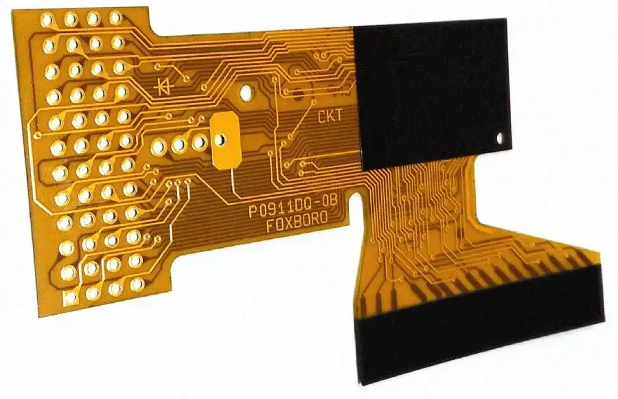
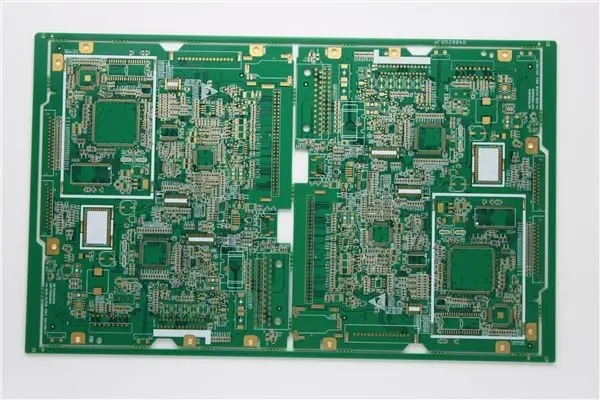
PCB制造
Judgment of PCB current and voltage feedback and solution of over dense solder joints
PCB manufacturers, PCB designers and PCBA manufacturers explain PCB current and voltage feedback judgment and the solution to over dense solder joints
First of all, the circuit board factory will learn the basIC points of the negative feedback amplifier circuit with you.
What is positive feedback? The positive feedback signal and our input signal have the same phase. When we add, it is very easy to have oscillations.
What is negative feedback? Negative feedback is to ensure that our amplification circuit can work normally within our operating range. Mining means that the feedback signal and the input signal of our amplification circuit are in opposite phases and subtract.
After that, let's return to our topic. Let's first look at what voltage feedback is.
The voltage feedback takes out the voltage of the output signal from the output terminal of the amplifier to stabilize the voltage of the output signal.
Voltage feedback judgment: if the output signal is cancelLED and there is no signal in the feedback, whether the sampling point and the output terminal are at the same point, if they are at the same point, they belong to voltage feedback and parallel circuit output terminal.
How to understand the SMAll output resistance of voltage feedback: it is conducive to understanding that the parallel voltage is equal everywhere and the parallel resistance becoMES smaller.
Circuit board factory summary: the sampling element of voltage feedback is parallel output terminal, and the output resistance is small.
We can see that the output terminal is fed back in parallel; It is determined that it is voltage feedback, and at the same time, the output signal is cancelled, and the feedback has no signal.
After seeing what voltage feedback is, let's take a look at current feedback.
Current feedback: it is to collect the signal current at the output end of our amplifier. As we know, the current of the series resistance is equal everywhere, and the series resistance is equal to the sum of all the resistances. We can use this to understand that current feedback is to connect the feedback elements in series at the output end of our feedback. Increase the value of the output resistance. At the same time, the feedback sampled signal is not at the same endpoint as our output.
The Circuit board factory and you can see that the RF sampling point and output terminal are different. They are connected in series to the sampling output resistor. When the output signal is cancelled, there is a signal coming (see the terminal is a negative signal).
circuit board factory summary: the voltage and current feedback is based on the output terminal of the amplifier. The voltage feedback reduces the output resistance, and the current feedback increases the output resistance.
Voltage feedback can stabilize the output voltage, reduce the output resistance, and improve the ability to drive the load.
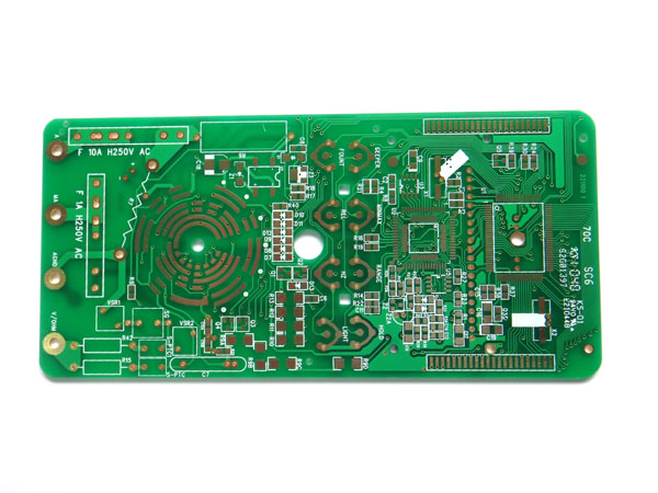
Solution to Solder Joint Overdensity in PCB Design
PCB PCB is designed with too dense solder joints, which is easy to cause wave soldering and electric leakage between solder joints. The following is a small compilation of PCB manufacturers to analyze the solution of excessive solder joints in PCB design.
Solution to Solder Joint Overdensity in PCB design
Analysis: This board has many plug-in components, which are relatively dense. Because the space between the solder joints is 0.3-0.5mm, it is easy to cause continuous welding. At the same time, because of the poor quality of the flux, a large amount of electric leakage occurs in the southern Meiyu weather.
Countermeasures: increase the welding spot spacing, and add welding resistance oil in the middle. Strictly control the quality of flux.
Consideration: When designing dense PCB boards, try to close them in a small area and open them where they can. For example, although the safe spacing of PCB is 0.3MM, the area where 0.6MM can be achieved should be increased to more than 0.6, so that the probability of problems will be greatly reduced.
PCB manufacturers, PCB designers and PCBA manufacturers will explain PCB current and voltage feedback judgment and the solution to over dense solder joints.


抖音二維碼

Q Q二維碼

微信二維碼
點擊
然后
聯系
然后
聯系
電話熱線
13410863085Q Q

微信

- 郵箱