鑫景福致力于滿足“快速服務,零缺陷,輔助研發(fā)”PCBA訂購單需求。


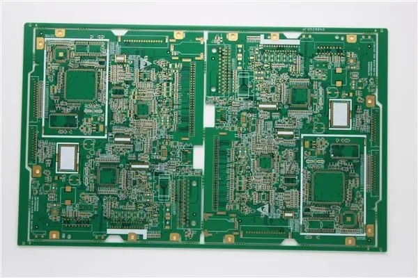
PCB制造
Causes of Wrinkle and Bubble of PCB welding Ink
The circuit board manufacturer, circuit board designer and PCBA processor explain the reasons for the wrinkling and bubbling of the circuit board welding ink
1. The cleanliness of the circuit board surface;
2. Surface mICro roughness (or surface energy). The blistering problem on the PCB surface of all circuit boards can be summarized as the above reasons. The binding force between the coatings is poor or too low, which makes it difficult to resist the coating stress, mechanical stress and thermal stress generated during the production and processing of PCB in the subsequent process of PCB production and assembly, resulting in different degrees of separation between the coatings.
Some factors that may cause poor board surface quality during production and processing are summarized as follows:
Problems of substrate processing: especially for some thin substrates (generally below 0.8mm), it is not suitable to use a brush because of the poor rigidity of the substrate. In this way, it may not be possible to effectively remove the protective layer specially treated to prevent the oxidation of the copper foil on the board surface during the production and processing of the substrate. Although this layer is thin and easy to remove by brushing, it is difficult to use chEMIcal treatment. Therefore, attention should be paid to control during the production and processing to avoid the blistering problem on the board surface caused by the poor adhesion between the copper foil and the chemical copper; When the thin inner layer is blackened, there will also be problems such as bad blackening and browning, uneven color, and poor local blackening and browning
2. Poor surface treatment caused by oil contamination or other liquid contamination during machining (drilling, laminating, milling, etc.) of circuit board surface.
3. Water washing problem: a large number of chemical solutions are required for copper plating treatment. There are many kinds of acid, alkali, non-polar organic and other pharmaceutical solvents, and the circuit board surface is not washed clean. In particular, the adjustment of degreaser for copper plating will not only cause cross contamination, but also cause local poor treatment or poor treatment effect, uneven defects, and cause some problems in the binding force; Therefore, attention should be paid to strengthening the control of water washing, mainly including the control of water flow, water quality, water washing time, and dripping time of the board; Especially in winter when the temperature is low, the washing effect will be greatly reduced, and more attention should be paid to the control of washing;
4. Poor copper plating brush plate: the pressure of the grinding plate before copper plating is too high, which causes the deformation of the orifice, brush out the copper foil round corner of the orifice, or even leak the base material at the orifice, which will cause blistering at the orifice in the process of copper plating, tin spraying, welding, etc; Even though the brush plate does not cause leakage of the base material, the overweight brush plate will increase the roughness of the copper at the orifice. Therefore, the copper foil at this place is very easy to coarsen during the micro etching process, and there will also be some quality risks; Therefore, attention should be paid to strengthening the control of the brush plate process, and the brush plate process parameters can be adjusted to the best through the abrasion test and water film test;
5. Micro etching in copper precipitation pretreatment and pattern electroplating pretreatment: excessive micro etching will cause base material leakage at the orifice, resulting in blistering around the orifice; Inadequate micro etching will also lead to insufficient bonding force, leading to blistering; Therefore, it is necessary to strengthen the control of micro etching; Generally, the micro etching depth of pretreatment for copper deposition is 1.5-2 μ m, and the micro etching depth of pretreatment for pattern electroplating is 0.3-1 μ m. If possible, it is better to control the micro etching thickness or etching rate through chemical analysis and SIMple test weighing method; Generally, the plate surface after micro etching has bright color, which is uniform pink, without reflection; If the color is uneven or there is reflection, it indicates that there is a potential quality hazard in the pre processing; Pay attention to strengthening inspection; In addition, the copper content, bath temperature, loading capacity and micro etchant content of the micro etching bath should be noted;
6. Poor reworking of copper sinking: some reworked plates after copper sinking or pattern transformation will blister due to poor fading, incorrect reworking method or improper control of micro etching time during reworking or other reasons; If poor copper deposition is found on the line for rework of copper plate, it can be directly reworked without corrosion after oil removal from the line directly after water washing; It is better not to degrease and slightly erode again; For the circuit board that has been electrically thickened, the micro etching groove shall be removed. Pay attention to the time control. You can roughly calculate the removal time with one or two boards to ensure the removal effect; After deplating, apply a group of soft grinding brushes behind the brush machine to brush lightly and then deposit copper according to the normal production process, but the etching and micro etching time shall be halved or adjusted as necessary; The Circuit board manufacturer, circuit board designer and PCBA processor explain the reasons for the wrinkling and bubbling of the circuit board welding ink.


抖音二維碼

Q Q二維碼

微信二維碼
點擊
然后
聯(lián)系
然后
聯(lián)系
電話熱線
13410863085Q Q

微信

- 郵箱