鑫景福致力于滿足“快速服務,零缺陷,輔助研發”PCBA訂購單需求。


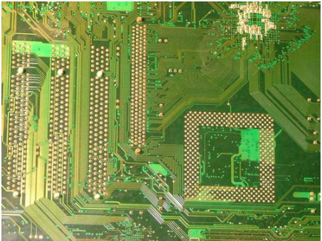
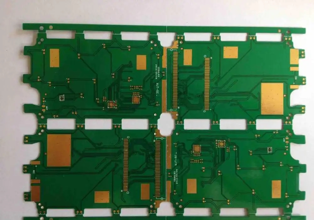
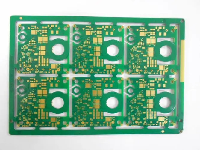
PCB制造
Pcb proofing has always been the main concern of the test engineer is to ensure that he has an effective test program, whICh can be well executed in production. In circuit testing (ICT) is still a very effective method to detect manufacturing defects. The more advanced ICT system can also add practical value in the test function configuration by providing the method of programming Flash memory, PLD, FPGA and EEPROM during the test. Agilent 3070 system is the MARKet leader in ICT.
Now ICT still plays an important role in the manufacturing and testing of printed circuit board assembly (PCA), but how will people's pursuit of lead-free PCB affect the ICT stage?
The promotion of lead-free soldering technology has LED to a lot of research on PCB surface treatment technology. These studies are mainly based on the technical performance in the PCB construction process. The impact of different PCB surface treatment technologies on the test phase is mostly ignored, or only focused on contact resistance. This report will provide details of the impacts observed in ICT and the need to respond to and understand these changes.
Experience in surface treatment of PCB proofing, and training for engineers to achieve changes in ICT PCB production process requirements. This paper will talk about the surface treatment of lead-free PCB, especially the ICT stage in the manufacturing process of, and reveal that the successful test of lead-free surface treatment also depends on the beneficial contribution of PCB construction process.
A successful ICT test is always based on the physical characteristics of the contact point between the test probe of the needle bed fixture and the test pad on the PCB. When a very sharp probe contacts a welded test point, the solder will sag because the contact pressure of the probe is much higher than the yield strength of the solder. As the solder sinks, the probe passes through any impurities on the surface of the test pad. The following uncontaminated solder now contacts the probe for good contact with the test point. The depth of probe insertion is a direct function of the yield strength of the target material. The deeper the probe penetrates, the better the contact.
An 8-ounce (oz) probe can apply a contact pressure of 26000 to 160000 psi (psi), depending on the surface diameter. Because the yield strength of solder is about 5000psi, the probe has better contact with this relatively soft solder.
Selection of pcb proofing surface treatment process
Before we understand the causes and consequences, it is important to describe the types of existing PCB surface treatment processes and what these types can provide. All printed circuit boards (PCBs) have copper layers on them. If the copper layer is not protected, it will be oxidized and damaged. There are many different protective layers available, the most common ones are hot air solder leveling (HASL), organic solder protection (OSP), electroless nickel gold immersion (ENIG), silver immersion and tin immersion.
Hot air solder leveling (HASL)
pcb proofing HASL is the main lead surface treatment process used in industry. The process is formed by immersing the circuit board into the lead tin alloy, and excessive solder is removed by the "wind knife", the so-called wind knife is the hot air blowing on the board surface. For PCA process, HASL has many advantages: it is the cheapest PCB, and the surface layer can also be welded after repeated reflow, cleaning and storage. For ICT, HASL also provides the process of automatically covering test pads and vias with solder. However, compared with the existing alternative methods, HASL surface has poor flatness or coplanarity. Now there are some lead-free HASL alternative processes, which are more and more popular due to the natural replacement of HASL. The application of HASL has achieved good results over the years, but with the emergence of "environmental protection" green process requirements, the existence of this process is numbered. In addition to the lead-free problem, the increasingly high board complexity and finer spacing have exposed many limitations of the HASL process.
Advantages: pcb proofing surface technology, which can maintain weldability throughout the manufacturing process, has no negative impact on ICT.
Disadvantages: Usually lead containing process is used, which is now limited and will be eliminated before 2007. For fine pin pitch (<0.64mm), it may lead to solder bridging and thickness problems. The unevenness of the surface will lead to the problem of the same surface in the assembly process.
Pcb proofing organic solder protective agent
Organic solder protective agent (OSP) is used to produce a thin, uniform and consistent protective layer on the copper surface of PCB. This coating protects the circuit from oxidation during storage and assembly operations. This process has existed for a long time, but it was not popularized until recently with the search for lead-free technology and fine pitch solutions.
OSP has better performance in PCA assembly than HASL in terms of the same plane and weldability, but requires significant process changes in the type of flux and the number of thermal cycles. Because its acidic characteristics will reduce the OSP performance and make copper easy to oxidize, it needs to be treated carefully. Assemblers prefer to deal with metal surfaces that are more flexible and can withstand more thermal cycles.
PCB proofing OSP surface treatment, if the test point is not welded, it will lead to the contact problem of the needle bed fixture in ICT. SIMply changing to a sharper probe type to pass through the OSP layer will only result in damage and puncture of the PCA test vias or test pads. The research shows that the higher probe force or the change of probe type has little effect on the yield. The yield strength of untreated copper is one order of magnitude higher than that of lead welding, and the only result is that the exposed copper test pad will be damaged. All testability guidelines strongly recommend that bare copper is not detected directly. When using OSP, you need to define a set of OSP rules for the ICT phase. The most important rule requires that Stencil be opened at the beginning of PCB process to allow solder paste to be added to the test pads and vias that ICT needs to contact.
Advantages: Comparable with HASL in unit cost, good coplanarity, lead-free process, and improved solderability.
Disadvantages: The assembly process needs to be greatly changed. If the unprocessed copper surface is detected, it will be bad for ICT. If the over sharp ICT probe may damage the PCB, manual preventive treatment is required, which limits ICT testing and reduces the repeatability of testing.
pcb
No electroplating nickel gold immersion for pcb proofing
The electroless nickel gold immersion (ENIG) coating has been successfully applied to many circuit boards. Although it has a high unit cost, it has a flat surface and excellent solderability. The main disadvantage is that the electroless nickel layer is very fragile and has been found to crack under mechanical pressure. This is called "black block" or "mud crack" in PCB industry, which has led to some negative reports of ENIG.
Advantages: good weldability, flat surface, long storage life, can withstand multiple reflow soldering.
Disadvantages: high cost (about 5 tiMES that of HASL), "black block" problem, cyanide and other harmful chEMIcals are used in PCB manufacturing process.
Pcb proofing silver immersion
Silver immersion is a newly added method for PCB surface treatment. It is mainly used in Asia and is being promoted in North America and Europe.
In the welding process, the silver layer melts into the welding point, leaving a tin/lead/silver alloy on the copper layer, which provides a very reliable welding point for BGA packaging. Its contrast color makes it easy to be checked, and it is also a natural alternative to HASL in welding treatment.
Silver immersion is a surface processing technology with a very good development prospect, but like all new surface processing technologies, the end user is very conservative about this. Many manufacturers regard this process as a "under investigation" PCB process, but it is likely to become the best lead-free surface process choice.


抖音二維碼

Q Q二維碼

微信二維碼
點擊
然后
聯系
然后
聯系
電話熱線
13410863085Q Q

微信

- 郵箱