鑫景福致力于滿足“快速服務,零缺陷,輔助研發”PCBA訂購單需求。


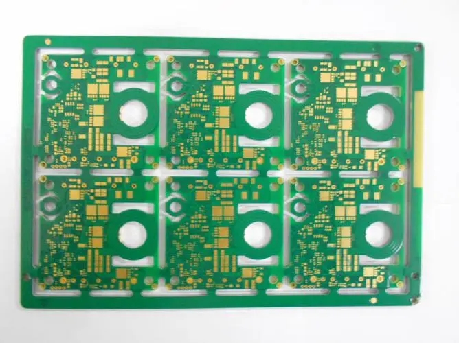
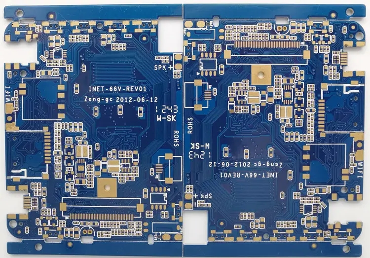
PCB制造
Why does PCB need to be gilded? What's the usage?
PCB manufacturers, PCB designers and PCBA manufacturers explain why PCB should be gilded? What's the usage?
1、 PCB board surface treatment
Oxidation resistance, tin spraying, lead-free tin spraying, gold deposition, tin deposition, silver deposition, hard gold plating, full plate gold plating, gold finger, nICkel palladium gold OSP: low cost, good solderability, harsh storage conditions, short time, environmentally friendly process, good welding and flatness. Tin spraying: tin spraying board is generally a multi-layer (4-46 layers) high-precision PCB template, which has been used by many large doMEStic communication, computer, Medical Equipment, aerospace enterprises and research institutions. The connecting finger is a connecting part between memory modules and memory sockets, and all signals are transmitted through the golden finger.
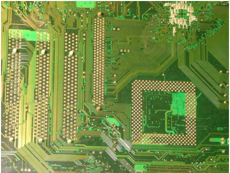
The golden finger is composed of many golden conductive contacts. Because its surface is gold-plated and the conductive contacts are arranged like fingers, it is calLED the "golden finger". Gold finger is actually coated with a layer of gold on the CCL through a special process, because gold has strong oxidation resistance and strong conductivity. However, due to the high price of gold, more memories are now replaced by tin plating. Tin materials have been popular since the 1990s. At present, the "golden finger" of mainboards, memories, graphics cards and other devices are almost all made of tin materials. Only some high-performance servers/workstations will continue to use the method of gold plating at their accessory contact points, which is naturally expensive.
2、 Why use gold plate
With the increasing integration of IC, the IC pins become more and more dense. The vertical tin spraying process is difficult to smooth the thin bonding pads, which makes it difficult to mount SMT; In addition, the shelf life of tin spraying plate is very short. The gold-plated board just solves these problems: 1. For the surface mount process, especially for 0603 and 0402 super SMAll surface mount, because the pad flatness is directly related to the quality of solder paste printing process, and plays a decisive role in the subsequent reflow welding quality, the whole board gold-plated is often seen in high-density and super small surface mount processes. 2. In the trial production stage, due to factors such as component procurement, it is often not that the plates are welded immediately when they arrive, but that they often wait for weeks or even months before being used. The shelf life of gold plated plates is many times longer than that of lead tin alloys, so everyone is willing to use them In addition, the cost of gold plated PCB in the sampling stage is almost the same as that of lead tin alloy plate. However, with the increasingly dense wiring, the line width and spacing have reached 3-4 MIL. Therefore, the problem of gold wire short circuit is brought: with the increasing frequency of the signal, the signal transmission in the multi coating due to skin effect has a more obvious impact on the signal quality. Skin effect refers to: high-frequency alternating current, the current will tend to concentrate on the surface of the wire flow. According to the calculation, the skin depth is related to the frequency.
3、 Why to use the gold plate
In order to solve the above problems of gold plated boards, PCB with gold plated boards mainly has the following characteristics:
Because the crystal structure formed by gold deposition and gold plating is different, the gold deposition will be golden yellow, which is more yellow than gold plating, and the customer is more satisfied.
2. Because the crystal structure formed by gold deposition is different from that formed by gold plating, gold deposition is easier to weld than gold plating, which will not cause poor welding and cause customer complaints.
3. Since only the pad of the gold plated plate has nickel gold, the signal transmission in the skin effect will not affect the signal in the copper layer.
4. Because the crystal structure of gold deposit is more compact than that of gold plating, it is not easy to produce oxidation.
5. Since only the bonding pad of the gold plate has nickel gold, it will not produce gold wire to cause slight shortness.
6. Since only the pad of the gold plated plate has nickel gold, the bonding between the solder mask and the copper layer on the circuit is stronger.
7. The project will not affect the spacing when making compensation.
8. Because the crystal structure formed by gold deposition and gold plating is different, the stress of the gold plate is easier to control, which is more conducive to the processing of bonding products. At the same time, because the gold is softer than the gold plating, the gold finger made of the gold plating plate is not wear-resistant.
9. The flatness and service life of the gold plated plate are as good as those of the gold plated plate.
4、 In fact, there are two gold plating processes for gold plate VS gold plate: one is electrogilding, the other is gold plating
For the gold plating process, the effect of tin coating is greatly reduced, while the effect of gold coating is better; Unless the manufacturer requires binding, most manufacturers will choose the gilding process now! Generally, PCB surface treatment is as follows: gold plating (electrogilding, gold deposition), silver plating, OSP, tin spraying (lead and lead-free). These are mainly for FR-4 or CEM-3 and other boards. The paper substrate is also coated with rosin; If the causes of poor tin coating (poor tin eating) are excluded from the production and material process of paster manufacturers such as solder paste.
Here, we only talk about PCB problems for the following reasons:
1. During PCB printing, whether there is an oil leakage film on the PAN position, which can block the effect of tin coating; This can be verified by tin bleaching test.
2. Whether the lubrication position of PAN position meets the design requirements, that is, whether the pad design can adequately ensure the support function of the parts.
3. If the pad is polluted, the result can be obtained by ion contamination test;
The above three points are basically the key aspects considered by PCB manufacturers. The advantages and disadvantages of several methods of surface treatment are that each has its own advantages and disadvantages! In terms of gold plating, it allows PCB to be stored for a long time, and has little change in temperature and humidity due to the external environment (compared with other surface treatments). Generally, it can be stored for about one year; Tin spraying surface treatment is followed by OSP. The storage time of these two surface treatments at ambient temperature and humidity should be paid attention to. In general, the surface treatment of silver is a little different, the price is also high, and the storage conditions are more demanding, so it needs to be packaged with sulfur free paper! And the storage time is about three months! In terms of tin coating effect, gold deposition, OSP, tin spraying, etc. are almost the same. The manufacturer mainly considers cost performance! PCB manufacturers, PCB designers and PCBA manufacturers explain why PCB should be gilded? What's the usage?


抖音二維碼

Q Q二維碼

微信二維碼
點擊
然后
聯系
然后
聯系
電話熱線
13410863085Q Q

微信

- 郵箱