鑫景福致力于滿足“快速服務,零缺陷,輔助研發”PCBA訂購單需求。


PCB制造
Three key processes in HDI PCB manufacturing
PCB manufacturing, PCB design, and PCBA processing manufacturers will explain the three key manufacturing processes in HDI PCB manufacturing
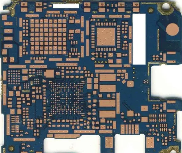
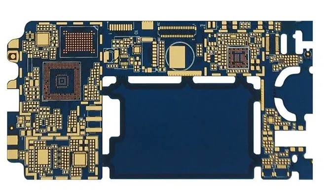
HDI board is a kind of precision circuit board in PCB board, and its board making process is also complex. The important steps include the formation of high-precision printed circuits, the processing of mICro through holes, and the electroplating of surfaces and holes. Next, let's take a look at these important steps in HDI PCB plate making.
1、 Ultra fine line processing
With the development of science and technology, some high-tech equipment is becoming SMAller and more precise, which requires higher and higher HDI boards.
The line width/line spacing of HDI circuit boards of some equipment has developed from 0.13 mm (5 mil) to 0.075 mm (3 mil), and has become the mainstream standard.
The higher and higher line width/line spacing requirements bring a direct challenge to the graphic imaging in PCB manufacturing process. How are the copper wires on these precision boards processed?
At present, the forming process of fine lines includes laser imaging (pattern transfer) and pattern etching.
Laser direct imaging (LDI) technology is to obtain fine circuit graphics directly from laser scanning on the surface of copper clad laminate coated with photoresist. Laser imaging technology SIMplifies the process flow and has become the mainstream technology in HDI PCB plate making.
Now the half addition method (SAP) and the improved half addition method (mSAP) are used more and more, that is, the graphic etching method. This technology can also realize the conductive circuit with a line width of 5um.
2、 Microporous processing
The important feature of HDI circuit board is that it has micro through holes (aperture ≤ 0.10 mm), which belong to buried blind hole structure.
At present, the buried blind holes on HDI boards are mainly processed by laser, but there are also CNC drilling holes.
Compared with laser drilling, mechanism drilling also has its own advantages. When laser processing the through hole of the epoxy glass cloth dielectric layer, the quality of the hole will be slightly poor due to the difference of the ablation rate between the glass fiber and the surrounding resin, and the residual glass fiber on the hole wall will affect the reliability of the through hole. Therefore, the advantages of mechanical drilling at this time are reflected. In order to improve the reliability and drilling efficiency of PCB boards, laser drilling and mechanical drilling technologies are steadily improving.
3、 Electroplating and surface finishing
How to improve the electroplating uniformity and deep hole plating ability in PCB manufacturing, and improve the reliability of the board. This depends on the continuous improvement of electroplating process, starting from the proportion of electroplating solution, equipment allocation, operation procedures and other aspects.
The ability of high frequency acoustic wave to accelerate etching; Permanganic acid solution can enhance the decontamination ability of the workpiece. High frequency sound waves will stir and add potassium permanganate electroplating solution with a certain proportion in the electroplating tank. This will help the plating solution flow into the hole evenly. Thus, the deposition ability and electroplating uniformity of copper electroplating are improved.
At present, the copper plating for blind holes is also mature, and copper filling for through holes with different apertures can be carried out. The two-step copper plating hole filling method can be suitable for through-hole with different aperture and high thickness diameter ratio. It has strong copper filling ability and can minimize the thickness of copper layer on the surface.
There are many options for finishing the final surface of PCB. Electroless nickel/gold (ENIG) and electroless nickel/palladium/gold (ENEPIG) are widely used on PCB.
ENIG and ENEPIG both have the same gold DIPping process, so it is important to select an appropriate gold dipping process for reliable installation welding or wire bonding. There are three types of gold leaching processes: standard displacement gold leaching, high efficiency gold leaching with limited nickel dissolution, and reduction reaction gold leaching with mixed mild reducing agents. The effect of gold leaching by reduction reaction is better.
For the problem that the nickel layer contained in ENIG and ENEPIG coatings is not conducive to high-frequency signal transmission and the formation of thin lines, surface treatment can be used and electroless palladium/catalytic gold (EPAG) can be used to replace ENEPIG to remove nickel, so as to reduce the metal thickness. PCB manufacturing, PCB design and PCBA processing manufacturers will explain the three key manufacturing processes in HDI PCB manufacturing.


抖音二維碼

Q Q二維碼

微信二維碼
點擊
然后
聯系
然后
聯系
電話熱線
13410863085Q Q

微信

- 郵箱