鑫景福致力于滿足“快速服務,零缺陷,輔助研發”PCBA訂購單需求。


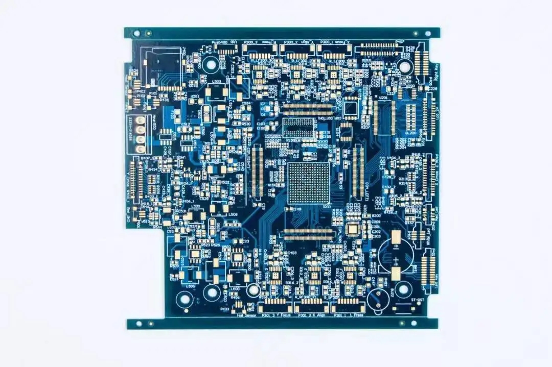
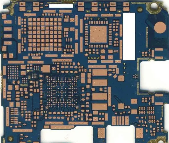
PCB制造
Why do photoelectrIC components on PCB always fail?
PCB manufacturers, PCB designers and PCBA manufacturers explain why the photoelectrIC components on PCB always fail?
As the carrier of various components and the hub of circuit signal transmission, PCB has become the most important and critical part of electronic information products. Its quality and reliability level determine the quality and reliability of the whole equipment.
With the miniaturization of electronic information products and the environmental requirements of lead-free and halogen-free, PCB is also developing towards high density, high Tg and environmental protection. However, due to the cost and technology, a large number of PCB failures have occurred in the production and application process, which has caused many quality disputes. In order to find out the causes of failure, find solutions to problems and clarify responsibilities, failure analysis must be carried out for the failure cases.
Basic procedure of failure analysis
In order to obtain the accurate cause or mechanism of PCB failure or defect, the basic principles and analysis process must be followed, otherwise valuable failure information may be missed, resulting in the analysis can not continue or may get wrong conclusions. The general basic process is to first determine the failure location and failure mode, that is, failure location or failure location, based on the failure phenomenon through information collection, functional test, electrical performance test and SIMple appearance inspection.
For simple PCB or PCBA, it is easy to determine the failure location. However, for more complex BGA or MCM packaged devices or substrates, the defects are not easy to observe through a microscope, which is not easy to determine at this time. At this time, it is necessary to use other means to determine.
Then we need to analyze the failure mechanism, that is, use various physical and chEMIcal means to analyze the mechanism that causes PCB failure or defect, such as faulty soldering, pollution, mechanical damage, wet stress, medium corrosion, fatigue damage, CAF or ion migration, stress overload, etc.
Then there is failure cause analysis, that is, based on failure mechanism and process analysis, find the cause of failure mechanism, and conduct test verification when necessary. Generally, test verification should be carried out as far as possible, and accurate causes of induced failure can be found through test verification.
This provides a targeted basis for further improvement. Finally, the failure analysis report is prepared according to the test data, facts and conclusions obtained in the analysis process. It is required that the facts in the report are clear, the logical reasoning is strict, and the organization is strong. Imagination is not allowed.
In the process of analysis, attention should be paid to the basic principles of using analytical methods from simple to complex, from outside to inside, from never destroying samples to using destruction. Only in this way can we avoid the loss of key information and the introduction of new artificial failure mechanisms.
Just like a traffic accident, if one party of the accident destroys or escapes from the scene, it is difficult for the sophisticated police to make an accurate responsibility determination. At this time, the traffic regulations generally require the person who escapes from the scene or the party who destroys the scene to assume full responsibility.
The same is true for failure analysis of PCB or PCBA. If an electric soldering iron is used to repair the faiLED solder joints or a large pair of scissors is used to cut the PCB forcefully, there is no way to start reanalysis. The failure site has been destroyed. Especially in the case of few failure samples, once the environment at the failure site is damaged or destroyed, the real failure cause cannot be obtained.
Failure Analysis Technology
optical microscope
The optical microscope is mainly used for the appearance inspection of PCB, to find the failure position and relevant physical evidence, and to preliminarily judge the failure mode of PCB. The appearance inspection mainly checks the PCB's contamination, corrosion, location of bursting, circuit wiring and regularity of failure, such as batch or individual, whether they are always concentrated in a certain area, etc.
X-ray (X-ray) For some parts that cannot be inspected by appearance, as well as the internal defects of PCB through-hole and other internal defects, X-ray fluoroscopy system must be used for inspection.
X-ray fluoroscopy system is to use different principles of moisture absorption or transmissivity of different materials with different thickness or density to image. This technology is more used to check the internal defects of PCBA solder joints, through hole internal defects and the positioning of defective solder joints of high-density BGA or CSP devices.
Slice analysis Slice analysis is the process of obtaining PCB cross section structure through a series of means and steps such as sampling, inlaying, slicing, polishing, corrosion and observation. Through slice analysis, we can get rich information about the microstructure of PCB (through-hole, coating, etc.), which provides a good basis for the next step of quality improvement. However, this method is destructive. Once sliced, the sample will be damaged.
At present, scanning acoustic microscope is mainly used for electronic packaging or assembly analysis, which is a C-mode ultrasonic scanning acoustic microscope. It uses the amplitude, phase and polarity changes generated by high-frequency ultrasonic reflection on the discontinuous interface of materials to image. Its scanning mode is to scan the X-Y plane information along the Z-axis.
Therefore, scanning acoustic microscope can be used to detect various defects in components, materials and PCB and PCBA, including cracks, delaminations, inclusions and cavities. If the frequency width of the scanning acoustic is sufficient, the internal defects of the solder joint can also be directly detected.
The typical scanning acoustic image shows the existence of defects in red warning color. Because a large number of plastIC encapsulated components are used in the SMT process, during the process of converting from lead to lead-free process, a large number of moisture reflux sensitive problems occur, that is, the hygroscopic plastic encapsulated devices will have internal or substrate delamination cracking when reflowing at higher lead-free process temperature, In the high temperature of lead-free process, the common PCB will often appear the phenomenon of board bursting.
At this point, the scanning acoustic microscope highlights its special advantages in nondestructive testing of multilayer high-density PCB. Generally, the obvious bursting plate can be detected by visual inspection.
Microscopic infrared analysis Microscopic infrared analysis is an analysis method that combines infrared spectrum and microscope. It uses the principle of different absorption of infrared spectrum by different materials (mainly organic substances) to analyze the compound composition of materials, and combines microscope to make visible light and infrared light have the same optical path. As long as you are in the visible field of view, you can find the trace organic pollutants to be analyzed.
If there is no combination of microscopes, usually infrared spectroscopy can only analyze samples with a large amount of samples. However, in many cases, micro contamination in electronic processes can lead to poor solderability of PCB pads or lead pins. It can be imagined that it is difficult to solve the process problem without the infrared spectrum matching the microscope. The main purpose of micro infrared analysis is to analyze the organic pollutants on the surface of the welded surface or solder joint, and analyze the causes of corrosion or poor weldability.
Scanning electron microscope analysis (SEM) Scanning electron microscope (SEM) is one of the most useful large electron microscopic imaging systems for failure analysis. It is most commonly used for morphology observation. At present, the function of scanning electron microscope is very powerful. Any fine structure or surface feature can be magnified to hundreds of thousands of tiMES for observation and analysis.
In terms of failure analysis of PCB or solder joint, SEM is mainly used to analyze the failure mechanism, specifically to observe the morphology and structure of the pad surface, the metallographic structure of the solder joint, measure intermetallics, analyze the solderable coating, and analyze and measure tin whiskers.
Unlike the optical microscope, the scanning electron microscope is an electronic image, so it is only black and white. In addition, the samples of the scanning electron microscope are required to conduct electricity, and the non conductors and some semiconductors need to be sprayed with gold or carbon, otherwise the observation of the samples will be affected if the charges accumulate on the surface of the samples. In addition, the depth of field of the scanning electron microscope image is far greater than that of the optical microscope, which is an important analysis method for the metallographic structure, micro fracture, tin whiskers and other uneven samples.
thermal analysis
Differential scanning calorimeter (DSC)
Differential scanning calorimetry (DSC) is a method to measure the relationship between the power difference between the input material and the reference material and the temperature (or time) under the programmed temperature control. It is an analytical method to study the relationship between heat and temperature. According to this relationship, the physical, chemical and thermodynamic properties of materials can be studied and analyzed.
DSC is widely used, but in PCB analysis, it is mainly used to measure the curing degree and glass transition temperature of various polymer materials used on PCB. These two parameters determine the reliability of PCB in the subsequent process.
Thermal Mechanical Analysis (TMA) is used to measure the deformation properties of solids, liquids and gel under the action of thermal or mechanical forces under the programmed temperature control. It is a method to study the relationship between thermal and mechanical properties. According to the relationship between deformation and temperature (or time), the physical, chemical and thermodynamic properties of materials can be studied and analyzed.
TMA is widely used in PCB analysis. It is mainly used for the two most critical parameters of PCB: measuring its linear expansion coefficient and glass transition temperature. PCB of base material with excessive expansion coefficient will often lead to fracture failure of metallized hole after welding and assembly.
Thermogravimetry Analysis (TGA) is a method to measure the relationship between the mass of substances and temperature (or time) under the programmed temperature control. TGA can monitor the subtle mass change of substances in the process of programmed temperature change through a precise electronic balance.
The physicochemical and thermodynamic properties of materials can be studied and analyzed according to the relationship between the mass of materials and temperature (or time). In terms of PCB analysis, it is mainly used to measure the thermal stability or thermal decomposition temperature of PCB materials. If the thermal decomposition temperature of the base material is too low, PCB will explode or delaminate at high temperatures during the welding process. PCB manufacturers, PCB designers and PCBA manufacturers explain why the photoelectric components on PCB always fail?


抖音二維碼

Q Q二維碼

微信二維碼
點擊
然后
聯系
然后
聯系
電話熱線
13410863085Q Q

微信

- 郵箱