鑫景福致力于滿足“快速服務,零缺陷,輔助研發”PCBA訂購單需求。


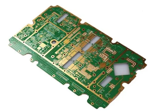
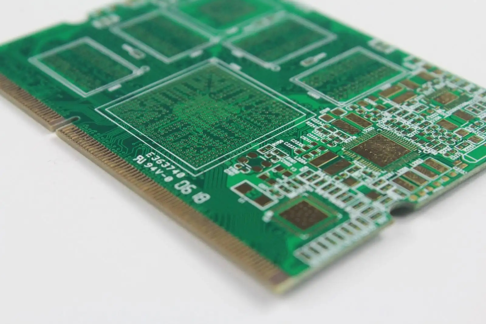
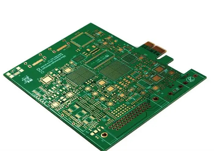
PCB制造
Introduction to Quality Control of Multilayer PCB Engineering Data
PCB manufacturing, PCB design and PCBA processing manufacturers will explain the quality control of multi-layer PCB engineering data
Quality Control of multilayer PCB Engineering Data
Any SMAll error in the engineering data may bring great loss to the production of multilayer PCB, and a SIMple processing skill of engineering data will greatly facilitate the production of multilayer PCB. Therefore, the quality of engineering data production can be improved by improving the requirements for engineering data production, standardizing the basIC contents and methods of engineering data processing, strengthening the systematic inspection of engineering data, and strengthening the rationalization of engineering data production process.
1 Requirements of multi-layer PCB production on engineering data
The engineering data of multilayer PCB board must provide convenience for production to the maximum extent on the basis of fully realizing the requirements of the designer, so that PCB manufacturers can achieve the design requirements more simply and safely. Therefore, the designer's requirements for PCB are the ultimate goal of engineering data production. The production of engineering data should make full use of existing equipment resources, processing methods and processing capabilities to achieve the technical requirements proposed by the design.
2. manufacturing process of multi-layer PCB engineering data
The production of engineering data is carried out on the CAD/CAM system. First, review the design content data of PCB Documents (including the highest number of layers, board thickness, minimum line width and line spacing, minimum finished product aperture, board outline dimension tolerance, aperture tolerance, special requirements, etc.) and Gerber format data conversion confirmed by CAM system; Secondly, on the prEMIse of ensuring PCB design requirements, according to the production capacity and process capacity of the production line, from the perspective of machinability, check and modify Gerber files on each layer of PCB and perform DRC check on Gerber files; Finally, the PCB graphic unit is automatically assembLED and CAM outputs the optimized photo drawing data, drilling and milling data, flying probe detection data, copper area for power supply plating and the preparation of manufacturing instructions.
3. Requirements for the production of multilayer PCB engineering data The engineering data for the production of multilayer PCB is the guiding process document for PCB production. On the one hand, it aims to achieve the design requirements, and on the other hand, it should meet the production capacity of the production line to the maximum extent.
3.1 Fabrication requirements for shape and panel data
The profile is made according to the PCB profile drawing provided by the design. The outline making rules are as follows.
(1) If there is no requirement in the design, the data shall be subject to the actual measurement in the document. If the data provided by the design or the data identification specified in the design document, check whether there is any contradiction in the data and whether the tolerance exceeds the capacity.
(2) The profile positioning requires 3 NPTH holes. The setting of profile positioning holes in the profile data should correspond to the positioning holes on the plate, and the positioning holes are not in a straight line.
(3) Large milling cutter shall be used as far as possible when milling the profile to reduce cutter breakage and improve the profile processing efficiency.
(4) For the bridge connecting plate, pay attention to the torque force generated by the splicing connection method, which may cause the failure to break completely after production.
(5) The profile data shall also include a profile processing instruction document, including the milling profile file name, milling cutter size, positioning hole tool size, and drilling positioning hole file name.
After the shape is determined, PCB units are assembled to ensure the minimum allowable size of PCB for each device and improve PCB production efficiency. The panel rules are as follows.
(1) Note that the spacing between graphic units should leave enough space for milling cutter, and the plate edge should be as small as possible, but should meet the requirements of electroplating, lamination and other processes on the plate edge.
(2) The improved circuit distribution is helpful for electroplating to disperse current and etching to reduce over etching.
(3) The boards with high alignment accuracy requirements such as high-rise counting boards and dense line boards should not be assembled into large boards.
(4) In order to reduce warpage, hot air leveling plates with plate thickness ≤ 1.2 mm should not be assembled into large plates.
(5) Gold finger board The gold finger is facing the outside of the board.
(6) Design of cutting size: length and width cannot be equal.
3.2 Requirements for making drilling data
If there is no special description in the design, the finished hole diameter and its tolerance shall be provided by the design, and the hole location, hole number and PTH/NPTH hole shall be MARKed. Make drilling documents according to the hole position in PCB graphics and the hole size requirements of the design.
(1) Check the double holes and stacked holes. If the hole diameters of multiple holes are consistent, delete them to only one hole. If the hole diameters are inconsistent, confirm the hole diameters of this hole location; If the hole stacking will lead to hole breaking, knife breaking, hot air leveling, hole bursting and other undesirable phenomena (except for stamp holes), ask the designer whether to add holes between the two holes or drill the two holes into grooves.
(2) Before the drilling file is generated, the requirements of the hole diameter tolerance and the influence of the copper plating process on the hole diameter must be compensated in the CAM system.
(3) Compare the drilling data with the profile data, check whether there is any hole that may be broken due to the intersection with the profile, and whether the positioning hole and the hole drilled with the profile are included in the drilling data; Compare the drilling data with the circuit diagram of each layer, and check whether the drilling may affect the electrical connection of the circuit, such as whether the hole breaks the wire or causes a short circuit.
(4) The distance between the drilling and positioning holes on the edge of the multilayer PCB board must be equal.
(5) Check the drilling data for production based on the drilling data of PCB file, check the drilling type and quantity, and check whether there are many holes and leaks. In addition to the drilling documents, the drilling data also includes the list of drill tool rows corresponding to the drilling documents, mainly including the size of the drill tool, the number of holes, etc.
3.3 Film Production requirements
3.3. 1 Production requirements of line layer film
The line layer film includes the inner and outer line films.
(1) For the designed non plated through-hole or the process hole added outside the PCB pattern, it is necessary to ensure that there is an isolation area between the inner circuit and the outer circuit pattern.
(2) Check the width of the welding ring, and properly compensate the pads with small welding rings. If there is a pad that cannot be enlarged to ensure the pad pitch, contact the designer to add a teardrop pad or lengthen a round pad or delete a non functional pad; The wire width and wire spacing shall be properly compensated according to the selected copper thickness.
(3) The slit that is easy to cause open circuit on the dry film line shall be filled; The grid of the outer circuit pattern that is easy to cause solder mask bubbles shall be treated; In order to reduce the uneven degree of the coating, the uneven distribution of the outer line should be modified.
(4) Open the power layer, stratum and point map at the same time, and check that there is at least one isolation panel on each hole position, otherwise the power layer and stratum are short circuited; Network generation is conducted for each layer of photo file. After generation, the grounding copper sheet is lit, and the copper sheet connected to the power supply should not be lit, otherwise, the circuit is short circuited; Normally, the bipolar devices will not have two pins on the same network.
(5) Whether there is a large copper sheet on one side. If there is one, the PCB file should be modified into a copper sheet or grid on both sides to avoid warping.
(6) There are narrow areas between the isolation strips in the design documents or the isolation panels are dense. Check whether there is an open circuit due to the compensation of isolation panels or thermal bonding pads.
(7) Check whether the end point of the printed wire of the design document is connected to the pad to prevent open circuit caused by shrinking the pad when the pad is modified by the project.
(8) The line graph of each layer that is too close to the contour line shall be moved.
(9) Add a choke block in the large area base material area of the external groove or internal groove. If the design wiring is uneven, it is recommended to add a choke block in the base material area to prevent white spots, warping and other undesirable phenomena.
(10) In order to achieve uniform electroplating, auxiliary electroplating blocks shall be added at the edge of each panel, panel gap, and groove in the unit, and care shall be taken not to cause copper exposure.
(11) If there are isolated reflective spots without copper ring, it is recommended to design copper ring to avoid spot dropping after etching.
3.3. 2 Requirements for production of resistance welding and character film
(1) Based on the solder mask graphics provided by the design, solder mask graphics shall be made according to the size of the pad in the processed circuit graphics. The size of solder mask graphics shall be larger than the corresponding circuit graphics to ensure that solder mask cannot be placed on the pad.
(2) When the distance between SMT pads is small and the design requires resistance welding between SMT pads, the resistance welding pattern of SMT pads should be smaller.
(3) The holes drilled on the PCB and the process holes added shall be provided with solder mask graphics larger than the drilling diameter to prevent the solder mask ink from entering the hole and causing smaller aperture size.
(4) The BGA through hole solder pad shall be provided with drilling files and solder plug holes.
(5) When the edge of solder mask is too close to the printed wire, the solder mask can be shrunk or cut; If it is too close to the copper sheet, the copper sheet can be cut while ensuring the electrical performance of PCB.
(6) Check whether the characters cross the solder mask pattern, and handle the cross part to prevent the characters from hanging or entering the hole.
(7) If there is a large tin surface on the characters, the characters can not be cut. It is required to first level the characters with hot air and then screen them.
4 Suggestions on the preparation of engineering data
4.1 Manufacturability modification of PCB files designed
Because designers are not necessarily familiar with PCB manufacturing, they seldom consider the difficulties of PCB manufacturing when designing PCB. In fact, some manufacturing problems can be avoided by modifying PCB graphIC design according to production process without changing PCB electrical performance.
4. 2 Pay attention to the requirements of the production process on the engineering data. The engineering data should be convenient for production. Only after the production inspection can we know whether the engineering data is convenient for production. In addition, some processing methods of some processes that are conducive to production should be timely applied to the production of engineering data, which is conducive to improving the usability of engineering data.
5 Conclusion
In a word, whether the engineering data can meet the process, production capacity and processability of the production line on the premise of ensuring the design requirements of multi-layer PCB is an important aspect of engineering production. Therefore, engineering personnel are required to be quite familiar with the process production capacity and enterprise standards of each process of the production line, and even have a certain degree of understanding of the operation process of each process, including when making engineering changes, only when they understand the whole process can they make correct changes and ensure that the changes are complete. With the different design requirements of PCB and the different process production capacity of production line, the specific production requirements of engineering data are also different, and the specific parameters used in the production and inspection process are continuously accumulated in the production process. PCB manufacturers, PCB designers and PCBA manufacturers will introduce the quality control of multi-layer PCB engineering materials.


抖音二維碼

Q Q二維碼

微信二維碼
點擊
然后
聯系
然后
聯系
電話熱線
13410863085Q Q

微信

- 郵箱