鑫景福致力于滿足“快速服務,零缺陷,輔助研發”PCBA訂購單需求。


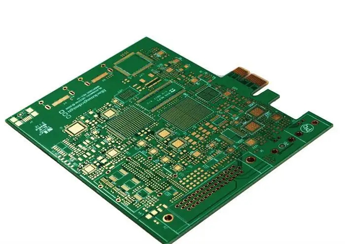
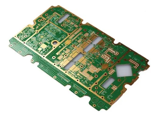
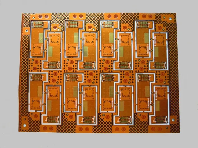
PCB制造
The PCB engineer tells you how to create a groove on a PCB
PCB manufacturing, PCB design and PCBA processing manufacturers explain to you how PCB engineers tell you how to create grooves on PCB boards
You can create pads with grooves and non round holes, and add grooves and square pad holes.
The detaiLED drilling type can be seen from the production and manufacturing steps. Place special string symbols on your PCB, add output instructions on it, and place legend string symbols on the DrillDrawing layer.
Note: If the latest software version supports the detection of output processing files, it is better to detect your PCB processing files and check whether there are grooves on your board. In addition, the methods commonly used in the earliest versions include the description of grooves in the mechanICal layer or the solder mask layer, using the text description method. Some designers will place pads or vias overlapped in the through-hole to define the drilling output area, but this may cause the drill bit to be damaged.
When the irregular hole manufacturing method is different from the next plate structure, you will find that your plate structure is more suitable for processing. There are therefore three ways to define grooves.
Add detailed processing information to the mechanical layer Add multi overlap pads or vias Apply CAMtasticNCDrill features
The details can be found in the PlatedRouteDetails of the mechanical layer, where you can see that the wiring connection is connected to the grooves of components J1, J6 and J2S. When switching to single-layer mode, you can see that the initial routing details of each layer (shortcut for switching to single-layer mode: shift, s) are included in the components, so the components will move when switching.
Before using this path, check the PCB processor to see if the method of setting dog talent can be accepted.
For this step, the pad and groove area must have been established with sufficient supporting information to the processor as follows:
Multi layer pads with holes are set to 0 units, which is the default setting that the pad starting and ending positions of the pad area are at the end of the groove position. The hole size set for these pads should be the same as the groove size.
Place a line from the starting center point to the pad on the mechanical layer of the coating channel details. The width of the line refers to the width of the groove cutting.
You also need to seriously consider the connection of the inner plane of the groove pad, and reserve enough space for the inner plane to place the solid connection, while the hot pad and the empty pad need to be manually set. In this PCB example, the thermal pad has been used - manually create arcs and lines, see Pad 1 of J6 for details
The power plane connection rules set for pads can be directly connected. As for design rules, check the power plane connection type setting rule settings to directly connect to these grooves. (Rules: PlaneConnect_Obround_Pads, adding a set class>class to the Pads in the design can be more easily set in the rules.) When assembling to the board, if you can't easily connect to the hot pads, you can select SIMple options to directly connect to these groove pads.
Finally, the groove pad cannot be connected to the plane. For example, pad 2 and pad 3 on J6 need to lay copper on the cut empty area, so add a line or other object as the flying wire of the shear area to connect the inner electric layer. Because the plane is negative output.
When you output your Gerber file or ODB++file, carefully check the connection of the internal electrical layer, remember to include the Plated routing details mechanical layer, and rEMInd your board manufacturer to pay attention to the groove pad on the PCB board. PCB manufacturing, PCB design and PCBA processing manufacturers explain to you how PCB engineers tell you how to create grooves on PCB boards.


抖音二維碼

Q Q二維碼

微信二維碼
點擊
然后
聯系
然后
聯系
電話熱線
13410863085Q Q

微信

- 郵箱