鑫景福致力于滿足“快速服務,零缺陷,輔助研發”PCBA訂購單需求。


行業新聞
Process Control Measures for SMT PCB Assembly Error
Surface Mount Technology (SMT) assembly is a popular installation technology in PCB manufacturing. Due to the quality of this technology in PCB manufacturing, it has been highly adopted by PCB contract manufacturers. However, with regard to the effICiency and reliability of PCB, some preventive measures must be taken in the manufacturing process These are calLED SMT PCB assembly process control measures These process control measures are smt pcb assembly processes defined for each step involved in the process In order to achieve quality, accuracy and prevent errors, process control measures must be taken This paper guides the process control measures for solder paste application to prevent smt pcb from being installed and soldered incorrectly
SMT PCB assembly process control measures
The following is a list of process control measures to be taken during the application of solder paste, component installation and reflow soldering.
Application of solder paste: The following process control measures shall be taken to avoid defects in solder paste printing or application.
Solder paste printing shall be consistent and uniform. Any deformation in the solder paste application may endanger the current distribution.
PCB pad oxidation shall be prevented.
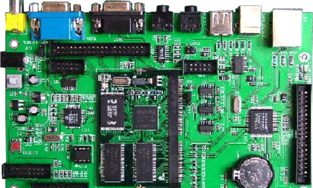
Circuit board

Prevent copper exposure or cross MARKing of copper traces.
Bridging, edge down, deviation, bending and twisting shall be prevented.
Printing shall be carried out from the core to the edge outward. The printing thickness shall be uniform.
The mounting holes on the template should match the reference marks on the circuit board. This ensures that the solder paste is used correctly without interrupting the component installation activities.
The mixing ratio of old solder paste and new solder paste should be 3:1
The application temperature of solder paste shall be kept at 25 ℃.
The relative humidity during solder paste printing should be between 35% and 75%.
After the solder paste is applied, automatic optical inspection (AOI), flying probe test, etc. shall be carried out. This can detect whether an error has occurred and help the site to correct it.
Assembly/wafer installation: Since wafer installation is completed by using automatic surface mounting device (SMD), the following precautions must be taken to avoid errors.
The SMD must be calibrated to the required chip installation function. Any error during SMD calibration may reflect the overall quality of PCB manufacturing.
Since SMD is automatically executed by computer code, careful programming, cross checking and editing are required to obtain the required results.
Feeders and SMDs shall be accurately installed and interconnected to prevent reoccurrence of errors.
Error detection, commissioning, troubleshooting and maintenance should be considered regularly. This helps prevent device deformation and device errors during the first cycle of chip installation. Before each wafer installation cycle, the settings must be debugged.
The relationship between device components and SMD operation paths must be analyzed.
Before carrying out the commissioning process, it is necessary to clarify the operation process. This facilitates results centric system calibration.
The redundancy of defects shall be analyzed to understand the recurrence of errors. Once the time period and location of the defect are known, the SMD can be calibrated accordingly.
Reflow soldering: Reflow soldering is the process of sinking the pasted flux and fixing the installed parts. The process needs to control temperature and other parameters.
The temperature curve, thermal curve, etc. must be analyzed in order to set the required melting temperature for reflow soldering.
The half moon shape of the solder joint shall be tested, as it can ensure a firm solder joint.
Check the PCB surface for any false soldering, bridging, solder paste or solder ball residue
Prevent vibration and mechanical shock during welding.


抖音二維碼

Q Q二維碼

微信二維碼
點擊
然后
聯系
然后
聯系
電話熱線
13410863085Q Q

微信

- 郵箱