鑫景福致力于滿足“快速服務,零缺陷,輔助研發”PCBA訂購單需求。


PCBA方案設計
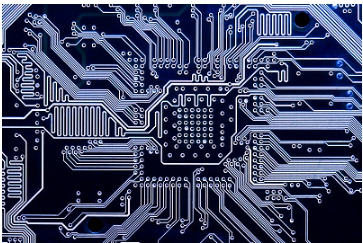
Analysis on Interference Generation of PCB Proofing 1 DSP System In order to make a stable and reliable DSP system, interference must be eliminated from all aspects, even if it cannot be completely eliminated, it must be minimized. For DSP system, the main interference coMES from the following aspects: ① Input and output channel interference. It means that the interference enters the system through the forward channel and the backward channel, such as the data acquisition link of the DSP system. The interference is superimposed on the signal through the sensor to increase the error of data acquisition. In the output link, the interference can increase the output data error, or even make a complete error, causing the system to collapse. Optocoupler devICes can be reasonably used to reduce the interference of input and output channels. For the interference of sensors and DSP main system, electrical isolation can be used to input positive interference. ② Interference of power supply system. The main interference source of the whole DSP system. The power supply not only provides power to the system, but also adds its noise to the power supply. The power line must be decoupLED when the power chip circuit is designed. ③ Space radiation coupling interference. The radiated coupling is often referred to as crosstalk. Crosstalk occurs in the electromagnetic field generated when the current flows through the wire, and the electromagnetic field induces transient current in the adjacent wire, causing adjacent signal distortion, or even error. The strength of crosstalk depends on the geometric dimensions and spacing of devices and wires. In DSP wiring, the greater the distance between signal lines and the closer to the ground wire, the more effective the crosstalk can be reduced. 2 Design PCB according to the cause of interference. The following is how to reduce various interference methods in the PCB manufacturing process of DSP system.
In order to improve the signal quality, reduce the difficulty of wiring, and increase the EMC of the system, the laminated design of multilayer boards is generally used in DSP high-speed digital circuits. The casCADe design can provide the shortest return path, reduce the coupling area and suppress differential mode interference. In the cascading design, special power layer and stratum are allocated, and the tight coupling of stratum and power layer is beneficial to the suppression of common mode interference (using adjacent planes to reduce the AC impedance of power plane). Take the 4-layer plate shown in Figure 1 as an example to illustrate the laminated design scheme. The structure designed with this 4-layer PCB has many advantages. There is a power supply layer below the top layer. The power supply pins of components can be directly connected to the power supply without passing through the ground plane. The key signals are laid on the bottom layer (bottom layer) to make more space for important signal routing, and the devices should be placed on the same layer as far as possible. If it is not necessary, do not make the board of two-layer parts, which will increase the assembly time and complexity. For example, the top layer, only when the top layer components are too dense, can devices with limited height and low heat generation, such as decoupling capacitors (patches), be placed on the bottom layer. For the DSP system, there may be a large number of lines to be laid, which can be laid in the inner layer by using the cascade design. If traditional through-hole will waste a lot of valuable cabling space, blind/buried via can be used to increase the cabling area.
In order to get the best performance of DSP system, the Layout of components is very important. DSP, Flash, SRAM and CPLD devices shall be placed first, and cabling space shall be carefully considered, then other ICs shall be placed according to the principle of functional independence, and finally I/O port shall be placed. Considering the size of PCB based on the above layout: if the size is too large, the printed line will be too long, the impedance will increase, the anti noise ability will decline, and the cost of board making will also increase; If the PCB is too SMAll, the heat dissipation is poor, and the space is limited, and adjacent lines are vulnerable to interference. Therefore, components shall be selected according to actual needs, and PCB size shall be generally calculated in combination with wiring space. When laying out the DSP system, pay special attention to the placement of the following devices.
(1) High speed signal is laid out in the whole DSP system. DSP, Flash and SRAM are the main high-speed digital signal lines. Therefore, the distance between devices should be as close as possible, and their connecting lines should be as short as possible and connected directly. Therefore, in order to reduce the impact of transmission lines on signal quality, high-speed signal routing should be as short as possible. Also consider that many DSP chips with speeds up to hundreds of MHz need to do snake winding. This will be highlighted in the cabling below.
(2) PCB digital analog device layout is not a single functional circuit in the DSP system. A large number of CM0S digital devices and digital analog hybrid devices are used, so digital/analog devices should be separated. The analog signal devices shall be concentrated as much as possible, so that the analog ground can draw an independent area belonging to the analog signal in the middle of the whole digital ground to avoid the interference of the digital signal to the analog signal. For some digital analog hybrid devices, such as D/A converter, it is traditionally regarded as an analog device, which is placed on the analog ground and provided with a digital loop, so that the digital noise can be fed back to the signal source to reduce the impact of digital noise on the analog ground.
(3) The clock layout shall be far away from I/O line and connector as far as possible for clock, chip selection and bus signal. The clock input of DSP system is easy to be disturbed, so its processing is very important. Always ensure that the clock generator is as close to the DSP chip as possible and that the clock line is as short as possible. The case of the clock crystal oscillator should preferably be grounded.
(4) Decoupling PCB layout In order to reduce the voltage transient overshoot on the power supply of the integrated circuit chip, a decoupling capacitor is added to the integrated circuit chip, which can effectively remove the impact of burrs on the power supply and reduce the power loop reflection on the PCB. Adding decoupling capacitors can bypass the high-frequency noise of integrated circuit devices, and can also be used as energy storage capacitors to provide and absorb the charging and discharging energy at the moment of opening and closing the doors of integrated circuits.
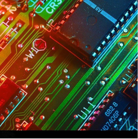
PCB proofing In the DSP system, place decoupling capacitors on each integrated circuit, such as DSP, SRAM, Flash, etc., and add them between each power supply and ground of the PCB chip. Pay special attention to that the decoupling capacitors should be as close as possible to the power supply end (source) and the part pin (pin) of the IC. Ensure the purity of the current from the power supply end (sotlrce end) and into the IC, and try to shorten the path of noise., When handling capacitors, large vias or multiple vias shall be used, and the connection between vias and capacitors shall be as short and thick as possible. When the two vias are far away, the path is too large, which is bad; The best thing is that the two vias of the decoupling capacitor are as close as possible, so that the noise can reach the ground with the shortest path.


抖音二維碼

Q Q二維碼

微信二維碼
點擊
然后
聯系
然后
聯系
電話熱線
13410863085Q Q

微信

- 郵箱